- 您現(xiàn)在的位置:買賣IC網(wǎng) > PDF目錄376420 > SPM3255 (Sanyo Electric Co.,Ltd.) Single Power Supply Operation RF Switch MMIC PDF資料下載
參數(shù)資料
| 型號: | SPM3255 |
| 廠商: | Sanyo Electric Co.,Ltd. |
| 英文描述: | Single Power Supply Operation RF Switch MMIC |
| 中文描述: | 單電源供電單片射頻開關(guān) |
| 文件頁數(shù): | 1/3頁 |
| 文件大小: | 30K |
| 代理商: | SPM3255 |

Any and all SANYO products described or contained herein do not have specifications that can handle
applications that require extremely high levels of reliability, such as life-support systems, aircraft’s
control systems, or other applications whose failure can be reasonably expected to result in serious
physical and/or material damage. Consult with your SANYO representative nearest you before using
any SANYO products described or contained herein in such applications.
SANYO assumes no responsibility for equipment failures that result from using products at values that
exceed, even momentarily, rated values (such as maximum ratings, operating condition ranges,or other
parameters) listed in products specifications of any and all SANYO products described or contained
herein.
Single Power Supply Operation
RF Switch MMIC
Ordering number:ENN6351
SPM3255
SANYO Electric Co.,Ltd. Semiconductor Company
TOKYO OFFICE Tokyo Bldg., 1-10, 1 Chome, Ueno, Taito-ku, TOKYO, 110-8534 JAPAN
12000GI (KT) No.6351–1/3
1
2
0
4
0
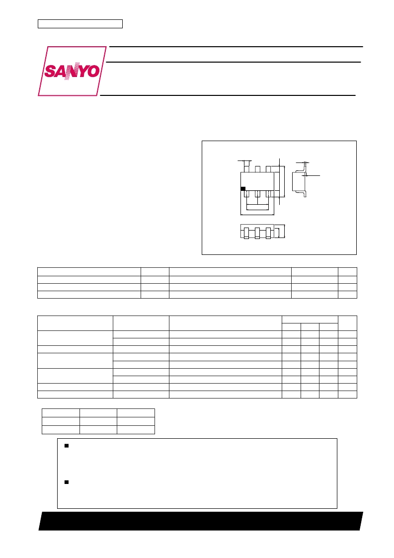
1.9
2.9
0.95 0.95
0
1
0.16
0.4
0 to 0.1
6
3
1
Specifications
Absolute Maximum Ratings
at Ta = 25C
Package Dimensions
unit:mm
1273
[SPM3255]
Features
· Control voltage +3 / 0V.
· Mini molded package.
· Low insertion loss, high linearity.
C
C
Electrical Characteristics
at Ta = 25C
1 : CTL – RX
2 : ANT
3 : CTL – TX
4 : TX
5 : GND
6 : RX
SANYO : CP6
r
m
a
P
l
b
m
y
S
s
n
o
n
o
C
s
g
n
R
t
U
e
e
p
e
p
m
g
a
V
T
e
g
l
o
g
S
n
p
O
C
V
T
T
L
T
C
g
r
o
5
0
0
V
m
e
e
T
5
7
1
+
+
o
0
5
2
5
–
–
o
r
m
a
P
l
b
m
y
S
s
+
n
o
n
a
v
o
C
)
V
0
/
3
e
g
l
o
C
(
s
g
n
R
y
t
U
n
m
p
x
a
5
9
5
m
s
s
o
L
n
o
s
n
X
X
R
R
–
–
T
T
N
N
A
A
,
N
,
N
A
X
T
N
A
–
N
A
–
N
A
–
N
A
–
w
A
–
X
A
–
–
,
X
X
X
X
X
X
X
s
T
T
R
T
T
T
T
T
T
z
H
M
3
3
0
1
z
z
1
z
1
z
z
H
H
o
H
G
G
o
0
G
o
0
1
G
9
=
1
8
=
1
8
=
0
1
8
9
9
1
8
9
8
=
=
=
=
=
=
B
B
A
B
B
d
d
μ
d
d
6
t
e
C
l
o
C
H
0
n
o
s
X
X
X
X
R
R
R
R
–
–
–
–
T
T
T
T
N
N
N
N
A
A
A
A
,
,
,
,
z
H
M
3
3
0
4
0
2
2
H
2
2
R
W
S
V
z
H
M
3
3
0
1
4
2
2
3
0
0
1
H
e
m
i
g
n
B
c
w
d
1
P
Marking : ML
S
z
z
H
H
G
G
9
9
o
o
M
M
0
0
0
0
0
s
m
B
n
X
R
–
T
N
A
,
N
z
7
1
d
X
T
–
L
T
C
X
R
–
L
T
C
V
3
+
V
0
X
T
→
T
N
A
V
0
V
3
+
T
N
A
→
X
R
相關(guān)PDF資料 |
PDF描述 |
|---|---|
| SPN03N60C3 | Cool MOS⑩ Power Transistor |
| SPN03N60S5 | Cool MOS⑩ Power Transistor |
| SPN03N60S5 | Cool MOS Small-Signal-Transistor(Cool MOS 小信號晶體管) |
| SPN04N60C2 | Cool MOS⑩ Power Transistor |
| SPN04N60S5 | Cool MOS⑩ Power Transistor |
相關(guān)代理商/技術(shù)參數(shù) |
參數(shù)描述 |
|---|---|
| SPM-32A | 制造商:JDSU 制造商全稱:JDS Uniphase Corporation 功能描述:Selective Level Meters |
| SPM32-CA | 制造商:FAIRCHILD 制造商全稱:Fairchild Semiconductor 功能描述:SPMTM (Smart Power Module) |
| SPM-33A | 制造商:JDSU 制造商全稱:JDS Uniphase Corporation 功能描述:Selective Level Meters |
| SPM-34A | 制造商:JDSU 制造商全稱:JDS Uniphase Corporation 功能描述:Selective Level Meters |
| SPM3501 | 制造商:SANYO 制造商全稱:Sanyo Semicon Device 功能描述:SPM3501 |
發(fā)布緊急采購,3分鐘左右您將得到回復(fù)。