- 您現(xiàn)在的位置:買賣IC網(wǎng) > PDF目錄297425 > SPT1019AIN (SIGNAL PROCESSING TECHNOLOGIES) PARALLEL, 8 BITS INPUT LOADING, 0.0055 us SETTLING TIME, 8-BIT DAC, PDIP24 PDF資料下載
參數(shù)資料
| 型號: | SPT1019AIN |
| 廠商: | SIGNAL PROCESSING TECHNOLOGIES |
| 元件分類: | DAC |
| 英文描述: | PARALLEL, 8 BITS INPUT LOADING, 0.0055 us SETTLING TIME, 8-BIT DAC, PDIP24 |
| 封裝: | PLASTIC, DIP-24 |
| 文件頁數(shù): | 8/12頁 |
| 文件大?。?/td> | 118K |
| 代理商: | SPT1019AIN |
SPT
5
5/14/97
SPT1019
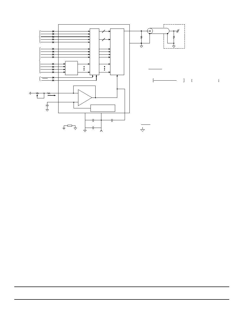
Figure 2 - Typical Interface Circuit
TYPICAL INTERFACE CIRCUIT
GENERAL
A typical interface circuit using the SPT1019 in a color raster
application is shown in figure 2. The SPT1019 requires few
external components and is extremely easy to use. The very
high operating speeds of the SPT1019 require good circuit
layout, decoupling of supplies, and proper design of trans-
mission lines. The following considerations should be noted
to achieve best performance.
INPUT CONSIDERATIONS
Video input data and controls may be directly connected to
the SPT1019. Note that all ECL inputs are terminated as
closely to the device as possible to reduce ringing, crosstalk
and reflections. A convenient and commonly used microstrip
impedance is about 130 ohms, which is easily terminated
using a 330 ohm resistor to VEE and a 220 ohm resistor to
Ground. This arrangement gives a Thevenin equivalent ter-
mination of 130 ohms to -2 volts without the need for a
-2 volt supply. Standard SIP (Single Inline Package) 220/330
resistor networks are available for this purpose. It is recom-
mended that stripline or microstrip techniques be used for all
ECL interface. Printed circuit wiring of known impedance
over a solid ground plane is recommended.
OUTPUT CONSIDERATIONS
The analog outputs are designed to directly drive a dual 50 or
75 ohm load transmission system as shown. The source
impedances of the SPT1019 outputs are high impedance
current sinks. The load impedance (RL) must be 25
or 37.5 ohms to attain standard RS-343-A video levels. Any
deviation from this impedance will affect the resulting video
output levels proportionally. As with the data interface, it is
important that the analog transmission lines have matched
impedance throughout, including connectors and transitions
between printed wiring and coaxial cable. The combination of
matched source termination resistor RS and load terminator
RL minimizes reflections of both forward and reverse travel-
ing waves in the analog transmission system. The return path
for analog output current is VCC which is connected to the
source termination resistor RS.
Output
Current
Switches
4 To 15
Decode
Video
Control
Inputs
Video
Data
Inputs
Clock
4
Ref
Buffer
ISet
FT
FH
Blank
BRT
Sync
D0 (LSB)
D1
D2
D3
D4
D5
D6
D7 (MSB)
CONV
Register
Video Monitor
Out+
R3
50/75
R4
50/75
50/75
COAX
Out-
Ref Out
COMP
All reference resistors 1/8 W 1% metal film power.
NOTES:
V- = -1.2 V (typical) for LM113.
V+ = -1.2 V
RL = R3 / / R4
K = 15.8069
K1 = 1.7617
K2 = 10.0392
FB = Ferrite bead, Fair-rite P/N 217430011 or equivalent.
1.
= ECL termination.
x
2.
3.
4.
6.
7.
8.
9.
ISet =
V+
αT(R
1+R2)
VOut- =
5.
VSync = (K x ISet x RL) + (K2 x ISet x RL)
supply decoupling 50 V ceramic disc.
255-Digital Input Code
255
x I Set
RL + KI x I Set x R L(Bright)
K
R2
750
V+
R1
500
ISet
Bandgap
Reference
10.
= VCC = AGND
11
.
See figure 8 for detail on Ref Buffer.
12. Ref Out on the SPT1019 can be used to drive up to
two SPT1018 reference inputs.
= DGND (digital input drivers).
VEE
VCC
-5.2 V
.01 F
10 F
13.
.01 F
C Comp
FB
.01 F
相關(guān)PDF資料 |
PDF描述 |
|---|---|
| SPT1019AIN | PARALLEL, 8 BITS INPUT LOADING, 0.0055 us SETTLING TIME, 8-BIT DAC, PDIP24 |
| SPT1019BIN | PARALLEL, 8 BITS INPUT LOADING, 0.0055 us SETTLING TIME, 8-BIT DAC, PDIP24 |
| SPT1019BIN | PARALLEL, 8 BITS INPUT LOADING, 0.0055 us SETTLING TIME, 8-BIT DAC, PDIP24 |
| SPT1175SCN | 8-BIT CONVERTER SUBSYSTEM ADC, PARALLEL ACCESS, PDIP24 |
| SPT1175SCU | 8-BIT CONVERTER SUBSYSTEM ADC, PARALLEL ACCESS, UUC24 |
相關(guān)代理商/技術(shù)參數(shù) |
參數(shù)描述 |
|---|---|
| SPT1019BIN | 制造商:CADEKA 制造商全稱:CADEKA 功能描述:8-BIT, HIGH SPEED D/A CONVERTER |
| SPT104 | 制造商:未知廠家 制造商全稱:未知廠家 功能描述:DC TO 1.1GHz LINEAR AMPLIFIER |
| SPT-105 | 功能描述:烙鐵 THERMOCOUPLE ASSEMB SP-100T/200T RoHS:否 制造商:Weller 產(chǎn)品:Soldering Stations 類型:Digital, Iron, Stand, Cleaner 瓦特:50 W 最大溫度:+ 850 F 電纜類型:US Cord Included |
| SPT-106 | 功能描述:烙鐵 CONTROL ASSEMBLY SP-100T RoHS:否 制造商:Weller 產(chǎn)品:Soldering Stations 類型:Digital, Iron, Stand, Cleaner 瓦特:50 W 最大溫度:+ 850 F 電纜類型:US Cord Included |
| SPT-108 | 制造商:Tamura Corporation of America 功能描述: |
發(fā)布緊急采購,3分鐘左右您將得到回復(fù)。