- 您現(xiàn)在的位置:買(mǎi)賣(mài)IC網(wǎng) > PDF目錄271689 > SPT674BCJ (SIGNAL PROCESSING TECHNOLOGIES) 1-CH 12-BIT SUCCESSIVE APPROXIMATION ADC, PARALLEL ACCESS, CDIP28 PDF資料下載
參數(shù)資料
| 型號(hào): | SPT674BCJ |
| 廠商: | SIGNAL PROCESSING TECHNOLOGIES |
| 元件分類: | ADC |
| 英文描述: | 1-CH 12-BIT SUCCESSIVE APPROXIMATION ADC, PARALLEL ACCESS, CDIP28 |
| 封裝: | SIDE BRAZED, CERAMIC, DIP-28 |
| 文件頁(yè)數(shù): | 10/12頁(yè) |
| 文件大小: | 103K |
| 代理商: | SPT674BCJ |

SPT
7
8/1/00
SPT674
The gain adjustment should be done at positive full scale. The
ideal input corresponding to the last code change is applied.
This is 1 and 1/2 LSB below the nominal full scale which is
+9.9963 V for the 10 V range and +19.9927 V for the 20 V
range. Adjust the gain potentiometer R2 for flicker between
codes 1111 1111 1110 and 1111 1111 1111. If calibration is
not necessary for the intended application, replace R2 with a
50
, 1% metal film resistor and remove the network from the
BIP OFF pin. Connect the BIP OFF pin to AGND. Connect the
analog input to the 10 V IN pin for the 0 to 10 V range or to the
20 V IN pin for the 0 to 20 V range.
BIPOLAR
The gain and offset errors listed in the specification may be
adjusted to zero using the potentiometers R1 and R2. (See
figure 6.) If adjustment is not needed, either or both pots may
be replaced by a 50
, 1% metal film resistor.
To calibrate, connect the analog input signal to the 10 V IN pin
for a
±5 V range or to the 20 V IN pin for a ±10 V range. First
apply a DC input voltage 1/2 LSB above negative full scale
which is -4.9988 V for the
±5 V range or -9.9976 V for
the
±10 V range. Adjust the offset potentiometer R1 for flicker
between output codes 0000 0000 0000 and 0000 0000 0001.
Next, apply a DC input voltage 1 and 1/2 LSB below positive
full scale which is +4.9963 V for the
±5 V range or +9.9927 V
for the
±10 V range. Adjust the gain potentiometer R2 for
flicker between codes 1111 1111 1110 and 1111 1111 1111.
The analog and digital common pins should be tied together
as close to the package as possible to guarantee best perfor-
mance. The code dependent currents flow through the VDD
terminal and not through the analog and digital common pins.
RANGE CONSIDERATIONS
The SPT674 may be operated by a microprocessor or in the
stand-alone mode. The part has four standard input ranges:
0 V to +10 V, 0 V to +20 V,
±5 V and ±10 V. The maximum
errors that are listed in the specifications for gain and offset
may be adjusted externally to zero as explained in the next
two sections.
CALIBRATION & CONNECTION PROCEDURES
UNIPOLAR
The calibration procedure consists of adjusting the
converter’s most negative output to its ideal value for offset
adjustment and then adjusting the most positive output to its
ideal value for gain adjustment.
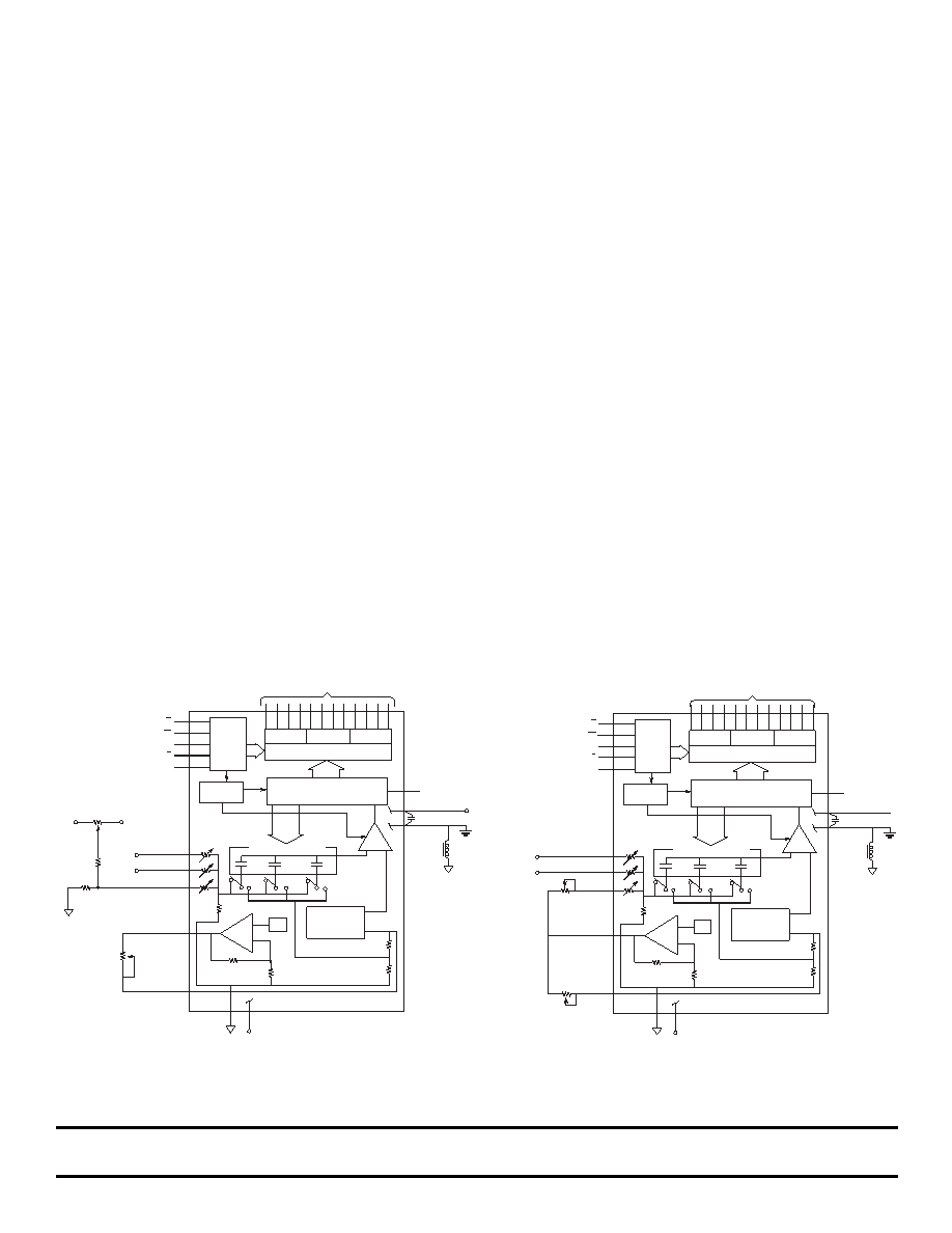
Starting with offset adjustment and referring to figure 5, the
midpoint of the first LSB increment should be positioned at
the origin to get an output code of all 0s. To do this, an input
of +1/2 LSB or +1.22 mV for the 10 V range and +2.44 mV for
the 20 V range should be applied to the SPT674. Adjust the
offset potentiometer R1 for code transition flickers between
0000 0000 0000 and 0000 0000 0001.
Figure 5 - Unipolar Input Connections
VRef In
Control
Logic
Nibble A
Nibble B
Nibble C
Three-State Buffers And Control
Oscillator
12-Bit SAR
12-Bits
Ref
Offset/Gain
Trim Network
Ref
Amp
Sample/Hold
Output Bits
VRef Out
BIP Off
20 V In
10 V In
STS
VDD
DGND
MSB
LSB
Strobe
Analog
Inputs
(Calibration)
.1 F
+5 V
R2
100
0 to 10 V
0 to 20 V
Ao
CE
CS
R/C
12/8
100 k
100 k
-15 V
+15 V
R1
100
CDAC
Comp
VEE
Control
Logic
Nibble A
Nibble B
Nibble C
Three-State Buffers And Control
Oscillator
12-Bit SAR
12-Bits
Ref
Offset/Gain
Trim Network
Ref
Amp
Sample/Hold
Output Bits
VRef Out
BIP Off
20 V In
10 V In
STS
VDD
DGND
MSB
LSB
Strobe
VRef In
Analog
Inputs
.1 F
+5 V
±5 V
±10 V
Ao
CE
CS
R/C
12/8
CDAC
Comp
100
R1
100
R1
VEE
Figure 6 - Bipolar Input Connections
相關(guān)PDF資料 |
PDF描述 |
|---|---|
| SD-14595D1-192Y | SYNCHRO OR RESOLVER TO DIGITAL CONVERTER, DIP36 |
| SD-14621DS-282S | SYNCHRO OR RESOLVER TO DIGITAL CONVERTER, CQIP54 |
| SDC-14604T-392 | SYNCHRO OR RESOLVER TO DIGITAL CONVERTER, DMA28 |
| SD-14531D1-424K | SYNCHRO OR RESOLVER TO DIGITAL CONVERTER, MDMA36 |
| SDC-14606-414L | SYNCHRO OR RESOLVER TO DIGITAL CONVERTER, DMA28 |
相關(guān)代理商/技術(shù)參數(shù) |
參數(shù)描述 |
|---|---|
| SPT674CCJ | 制造商:未知廠家 制造商全稱:未知廠家 功能描述:FAST, COMPLETE 12-BIT uP COMPATIBLE A/D CONVERTER WITH SAMPLE/HOLD |
| SPT68H-113 | 制造商:Coilcraft Inc 功能描述:Power inductor, toroid, 20% tol, SMT, RoHS |
| SPT68H-113ML | 制造商:Coilcraft Inc 功能描述:Power inductor, toroid, 20% tol, SMT, RoHS |
| SPT68H-113MLB | 功能描述:固定電感器 Power Inductor 11 uH 20 % 11.2 A RoHS:否 制造商:AVX 電感:10 uH 容差:20 % 最大直流電流:1 A 最大直流電阻:0.075 Ohms 工作溫度范圍:- 40 C to + 85 C 自諧振頻率:38 MHz Q 最小值:40 尺寸:4.45 mm W x 6.6 mm L x 2.92 mm H 屏蔽:Shielded 端接類型:SMD/SMT 封裝 / 箱體:6.6 mm x 4.45 mm |
| SPT68H-113MLD | 功能描述:固定電感器 Power Inductor 11 uH 20 % 11.2 A RoHS:否 制造商:AVX 電感:10 uH 容差:20 % 最大直流電流:1 A 最大直流電阻:0.075 Ohms 工作溫度范圍:- 40 C to + 85 C 自諧振頻率:38 MHz Q 最小值:40 尺寸:4.45 mm W x 6.6 mm L x 2.92 mm H 屏蔽:Shielded 端接類型:SMD/SMT 封裝 / 箱體:6.6 mm x 4.45 mm |
發(fā)布緊急采購(gòu),3分鐘左右您將得到回復(fù)。