- 您現(xiàn)在的位置:買賣IC網(wǎng) > PDF目錄271781 > SPT7861SCU (FAIRCHILD SEMICONDUCTOR CORP) 1-CH 10-BIT SUCCESSIVE APPROXIMATION ADC, PARALLEL ACCESS, UUC28 PDF資料下載
參數(shù)資料
| 型號: | SPT7861SCU |
| 廠商: | FAIRCHILD SEMICONDUCTOR CORP |
| 元件分類: | ADC |
| 英文描述: | 1-CH 10-BIT SUCCESSIVE APPROXIMATION ADC, PARALLEL ACCESS, UUC28 |
| 封裝: | DIE-28 |
| 文件頁數(shù): | 4/8頁 |
| 文件大?。?/td> | 91K |
| 代理商: | SPT7861SCU |
SPT
4
2/10/98
SPT7861
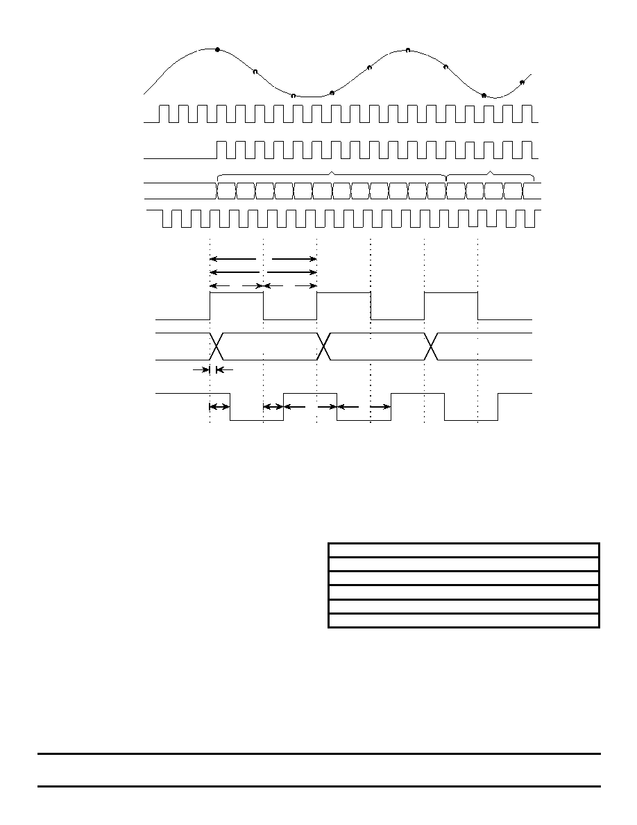
Figure 1A: Timing Diagram 1
Figure 1B: Timing Diagram 2
ANALOG IN
CLOCK IN
1
3
5
7
9
11
13
15
17
SAMPLING
CLOCK
(Internal)
DATA OUTPUT
DATA VALID
VALID
INVALID
13
24
5
tOD
tCL
tCH
tC
tCLK
Data
Data 1
Data 2
Data 3
CLOCK IN
DATA
OUTPUT
DATA
VALID
tS
tCH
tCL
tS
The high sample rate is achieved by using multiple SAR ADC
sections in parallel, each of which samples the input signal in
sequence. Each ADC uses 16 clock cycles to complete a
conversion. The clock cycles are allocated as follows:
Table II - Clock Cycles
Clock
Operation
1
Reference zero sampling
2
Auto-zero comparison
3
Auto-calibrate comparison
4
Input sample
5-15
11-bit SAR conversion
16
Data transfer
The 16 phase clock, which is derived from the input clock,
synchronizes these events. The timing signals for adjacent
ADC sections are shifted by one clock cycle so that the analog
input is sampled on every cycle of the input clock by exactly
one ADC section. After 16 clock periods, the timing cycle
repeats. The latency from analog input sample to the corre-
sponding digital output is 12 clock cycles.
TYPICAL INTERFACE CIRCUIT
Very few external components are required to achieve the
stated device performance. Figure 2 shows the typical inter-
face requirements when using the SPT7861 in normal circuit
operation. The following sections provide descriptions of the
major functions and outline critical performance criteria to
consider for achieving the optimal device performance.
POWER SUPPLIES AND GROUNDING
SPT suggests that both the digital and the analog supply
voltages on the SPT7861 be derived from a single analog
supply as shown in figure 2. A separate digital supply should
be used for all interface circuitry. SPT suggests using this
power supply configuration to prevent a possible latch-up
condition on power up.
OPERATING DESCRIPTION
The general architecture for the CMOS ADC is shown in the
block diagram. The design contains 16 identical successive
approximation ADC sections (all operating in parallel), a 16-
phase clock generator, an 11-bit 16:1 digital output multi-
plexer, correction logic, and a voltage reference generator
which provides common reference levels for each ADC section.
相關(guān)PDF資料 |
PDF描述 |
|---|---|
| SD-14621DS-425K | SYNCHRO OR RESOLVER TO DIGITAL CONVERTER, CQIP54 |
| SD-14552DX-524K | SYNCHRO OR RESOLVER TO DIGITAL CONVERTER, CQIP34 |
| SD-14552DX-544Q | SYNCHRO OR RESOLVER TO DIGITAL CONVERTER, CQIP34 |
| SD-14621FX-242Z | SYNCHRO OR RESOLVER TO DIGITAL CONVERTER, CDMA54 |
| SD-14621FX-104L | SYNCHRO OR RESOLVER TO DIGITAL CONVERTER, CDFP54 |
相關(guān)代理商/技術(shù)參數(shù) |
參數(shù)描述 |
|---|---|
| SPT7862 | 制造商:CADEKA 制造商全稱:CADEKA 功能描述:10-BIT, 40 MSPS, DUAL-CHANNEL A/D CONVERTER |
| SPT7862SIT | 制造商:CADEKA 制造商全稱:CADEKA 功能描述:10-BIT, 40 MSPS, DUAL-CHANNEL A/D CONVERTER |
| SPT7863 | 制造商:FAIRCHILD 制造商全稱:Fairchild Semiconductor 功能描述:10-BIT, 40 MSPS, 160 mW A/D CONVERTER |
| SPT7863SCS | 功能描述:直流/直流開關(guān)轉(zhuǎn)換器 10BIT 40MSPS SaR aDC RoHS:否 制造商:STMicroelectronics 最大輸入電壓:4.5 V 開關(guān)頻率:1.5 MHz 輸出電壓:4.6 V 輸出電流:250 mA 輸出端數(shù)量:2 最大工作溫度:+ 85 C 安裝風(fēng)格:SMD/SMT |
| SPT7863SCSX | 功能描述:直流/直流開關(guān)轉(zhuǎn)換器 RoHS:否 制造商:STMicroelectronics 最大輸入電壓:4.5 V 開關(guān)頻率:1.5 MHz 輸出電壓:4.6 V 輸出電流:250 mA 輸出端數(shù)量:2 最大工作溫度:+ 85 C 安裝風(fēng)格:SMD/SMT |
發(fā)布緊急采購,3分鐘左右您將得到回復(fù)。