- 您現(xiàn)在的位置:買賣IC網(wǎng) > PDF目錄373505 > SST111 (LINEAR INTEGRATED SYSTEMS INC) SINGLE N-CHANNEL JFET PDF資料下載
參數(shù)資料
| 型號: | SST111 |
| 廠商: | LINEAR INTEGRATED SYSTEMS INC |
| 元件分類: | 小信號晶體管 |
| 英文描述: | SINGLE N-CHANNEL JFET |
| 中文描述: | N-CHANNEL, Si, SMALL SIGNAL, JFET |
| 封裝: | SOT-23, 3 PIN |
| 文件頁數(shù): | 1/1頁 |
| 文件大小: | 21K |
| 代理商: | SST111 |
N-Channel JFET Swtch
J111 - J113 /SST111 – SST113
FEATURES
Low Cost
Automated Insertion Package
Low Insertion Loss
No Offset or Error Voltage Generated By Closed Switch
-
Purely Resistive
-
High Isolation Resistance From Driver
Fast Switching
Short Sample and Hold Aperture Time
APPLICATIONS
Analog Switches
Choppers
Commutators
ABSOLUTE MAXIMUM RATINGS
(T
A
= 25
o
C unless otherwise specified)
Gate-Drain or Gate-Source Voltage . . . . . . . . . . . . . . . . -35V
Gate Current . . . . . . . . . . . . . . . . . . . . . . . . . . . . . . . . . 50mA
Storage Temperature Range . . . . . . . . . . . . . -55
o
C to +150
o
C
Operating Temperature Range . . . . . . . . . . . -55
o
C to +135
o
C
Lead Temperature (Soldering, 10sec). . . . . . . . . . . . . +300
o
C
Power Dissipation . . . . . . . . . . . . . . . . . . . . . . . . . . . 360mW
Derate above 25
o
C . . . . . . . . . . . . . . . . . . . . . . 3.3mW/
o
C
NOTE:
Stresses above those listed under "Absolute Maximum
Ratings" may cause permanent damage to the device. These are
stress ratings only and functional operation of the device at these or
any other conditions above those indicated in the operational sections
of the specifications is not implied. Exposure to absolute maximum
rating conditions for extended periods may affect device reliability.
ORDERING INFORMATION
Part
J111-113
SST111-113
For Sorted Chips in Carriers see 2N4391 series.
Package
Plastic SOT-23
Plastic SOT-23
Temperature Range
-55
o
C to +135
o
C
-55
o
C to +135
o
C
C ORPORATION
PIN CONFIGURATION
5001
ELECTRICAL CHARACTERISTICS
(T
A
= 25
o
C unless otherwise specified)
SYMBOL
PARAMETER
111
TYP MAX MIN
-1
-10
112
TYP MAX MIN
-1
-5
113
TYP MAX
UNITS
TEST CONDITIONS
MIN
I
GSSR
V
GS(off)
BV
GSS
I
DSS
I
D(off)
r
DS(on)
C
dg(off)
Gate Reverse Current (Note 1)
Gate Source Cutoff Voltage
Gate Source Breakdown Voltage
Drain Saturation Current (Note 2)
Drain Cutoff Current (Note 1)
Drain Source ON Resistance
Drain Gate OFF Capacitance
-1
-3
nA
V
DS
= 0V, V
GS
= -15V
V
DS
= 5V, I
D
= 1
μ
A
V
DS
= 0V, I
G
= -1
μ
A
V
DS
= 15V, V
GS
= 0V
V
DS
= 5V, V
GS
= -10V
V
DS
= 0.1V, V
GS
= 0V
V
DS
= 0,
V
GS
= -10V
(Note 3)
V
DS
= V
GS
= 0
(Note 3)
Switching Time Test
Conditions (Note 3)
J111
V
DD
10V
V
GS(off)
-12V
R
L
0.8k
-3
-35
20
-1
-35
5
-0.5
-35
2
V
mA
nA
1
30
5
1
50
5
1
100
5
pF
f = 1MHz
C
sg(off)
Source Gate OFF Capacitance
5
5
5
C
dg(on)
+ C
sg(on)
t
d(on)
t
r
t
d(off)
Drain Gate Plus Source Gate ON
Capacitance
Turn On Delay Time
Rise Time
Turn Off Delay Time
28
28
28
7
6
20
7
6
20
7
6
20
ns
J112
10V
-7V
1.6k
J113
10V
-5V
3.2k
t
f
Fall Time
15
15
15
NOTES: 1.
Approximately doubles for every 10
o
C increase in T
A
.
2.
Pulse test duration 300
μ
s; duty cycle
≤
3%.
3.
For design reference only, not 100% tested.
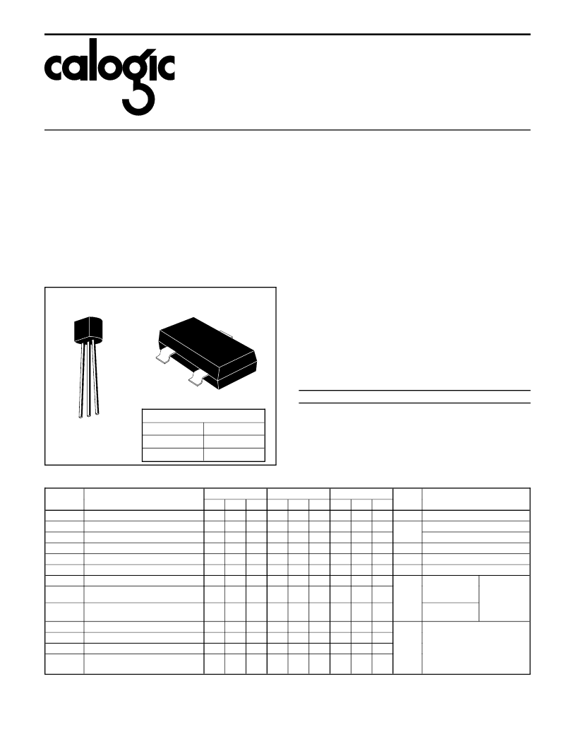
SOT-23
G
S
D
TO-92
SG
D
PRODUCT MARKING (SOT-23)
SST111
111
SST112
112
SST113
113
CALOGIC CORPORATION
, 237 Whitney Place, Fremont, California 94539, Telephone: 510-656-2900, FAX: 510-651-1076
相關(guān)PDF資料 |
PDF描述 |
|---|---|
| SST174 | P-Channel JFET Switch |
| SST175 | P-Channel JFET Switch |
| SST176 | P-Channel JFET Switch |
| SST177 | P-Channel JFET Switch |
| SST174 | SINGLE P-CHANNEL JFET SWITCH |
相關(guān)代理商/技術(shù)參數(shù) |
參數(shù)描述 |
|---|---|
| SST111_SOT-23 | 制造商:MICROSS 制造商全稱:MICROSS 功能描述:N-CHANNEL JFET |
| SST11-12FR-0 | 制造商:NA 功能描述: |
| SST111-E3 | 功能描述:JFET 55V 20mA RoHS:否 制造商:ON Semiconductor 晶體管極性:N-Channel 漏極電流(Vgs=0 時的 Idss):50 mA 漏源電壓 VDS:15 V 閘/源擊穿電壓: 漏極連續(xù)電流:50 mA 配置: 安裝風(fēng)格: 封裝 / 箱體:SC-59 封裝:Reel |
| SST111-T1 | 功能描述:JFET 55V 20mA RoHS:否 制造商:ON Semiconductor 晶體管極性:N-Channel 漏極電流(Vgs=0 時的 Idss):50 mA 漏源電壓 VDS:15 V 閘/源擊穿電壓: 漏極連續(xù)電流:50 mA 配置: 安裝風(fēng)格: 封裝 / 箱體:SC-59 封裝:Reel |
| SST111-T1-E3 | 功能描述:JFET 55V 20mA RoHS:否 制造商:ON Semiconductor 晶體管極性:N-Channel 漏極電流(Vgs=0 時的 Idss):50 mA 漏源電壓 VDS:15 V 閘/源擊穿電壓: 漏極連續(xù)電流:50 mA 配置: 安裝風(fēng)格: 封裝 / 箱體:SC-59 封裝:Reel |
發(fā)布緊急采購,3分鐘左右您將得到回復(fù)。