- 您現(xiàn)在的位置:買賣IC網(wǎng) > PDF目錄358382 > ST1318BGB-FREQ2(T) (PERICOM SEMICONDUCTOR CORP) VCXO, CLOCK, 80 MHz - 125 MHz, HCMOS/TTL OUTPUT PDF資料下載
參數(shù)資料
| 型號: | ST1318BGB-FREQ2(T) |
| 廠商: | PERICOM SEMICONDUCTOR CORP |
| 元件分類: | XO, clock |
| 英文描述: | VCXO, CLOCK, 80 MHz - 125 MHz, HCMOS/TTL OUTPUT |
| 文件頁數(shù): | 1/2頁 |
| 文件大?。?/td> | 119K |
| 代理商: | ST1318BGB-FREQ2(T) |

DS-171 REV C
SaRonix
SaRonix
Voltage Controlled Crystal Oscillator
Technical Data
S1318 / S1518 Series
3.3 & 5V, HCMOS, SMD
141 Jefferson Drive Menlo Park, CA 94025 USA 650-470-7700 800-227-8974 Fax 650-462-9894
Frequency Range:
32 MHz to 125 MHz
Frequency Stability:
ACTUAL SIZE
Description
A voltage controlled, low current crystal
oscillator, providing precise rise and fall
times to drive high performance applica-
tions. The device is packaged in a 6-pin,
SMD, J-leaded package. The plastic mold-
ed surface mountable package is ideal for
today's automated assembly environ-
ments.
Applications
For use in phase-locked loop (PLL)
clock and data recovery, frequency
translation, or frequency synthesis ap-
plications in video, video compression,
telephony, and LAN/WAN data com-
munication environments.
High and wide frequency range from
32 MHz to 125 MHz
3.3 or 5 Volt operation
Compact, plastic molded surface mount
package
HCMOS and TTL compatible
Tri-state output
Available on tape & reel; 24mm tape,
500pcs per reel
* APR = (VCXO Pull relative to specified Output Freq. @
nominal control voltage) – (VCXO Freq. Stability)
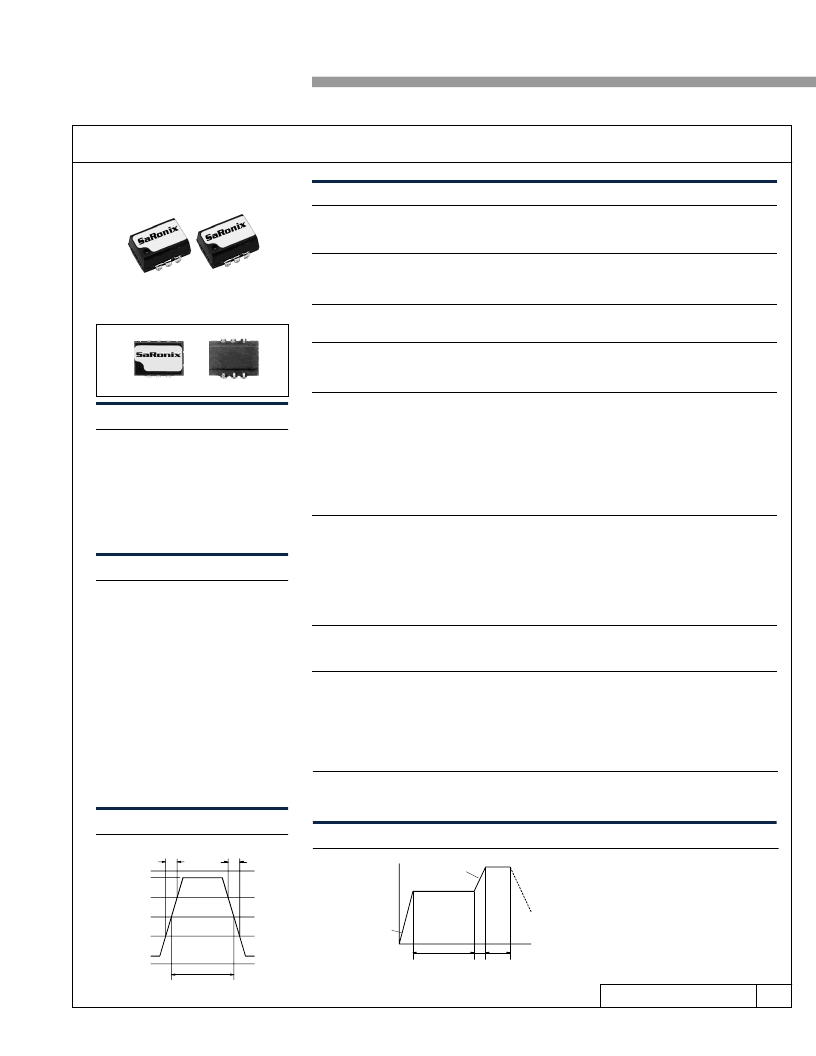
Output Waveform
T
r
T
f
HCMOS
SYMMETRY
1 LEVEL
80% V
DD
50% V
DD
20% V
DD
0 LEVEL
Input Impedance:
Frequency Response (-3dB):
Pullability:
Control Voltage:
Transfer Function:
Linearity:
Center Control Voltage:
50K
min
50 kHz min
±25, ±50, ±75 ppm APR* (See Part Numbering Guide)
0.5 to 4.5V, 0.3 to 3.0V
Frequency Increases when Control Voltage Increases
10% max
2.5V @ 5V or 1.65V @ 3.3V
Shock:
Solderability:
Terminal Strength:
Vibration:
Solvent Resistance:
Resistance to Soldering Heat:
Mechanical:
MIL-STD-883, Method 2002, Condition B
MIL-STD-883, Method 2003
MIL-STD-202, Method 211, Conditions A & C
MIL-STD-883, Method 2007, Condition A
MIL-STD-202, Method 215
MIL-STD-202, Method 210, Condition I or J
MIL-STD-883, Method 1011, Condition A
MIL-STD-883, Method 1004
Environmental:
Thermal Shock:
Moisture Resistance:
10 sec max
±50 ppm over all conditions: operating temperature, voltage change,
load change, calibration tolerance, aging, with V
C
= 2.5V @ 5V,
V
C
= 1.65V @ 3.3V
Temperature Range:
Operating:
Storage:
0 to +70°C, -40 to +85°C
-55 to +125°C
Supply Voltage:
Recommended Operating:
+5 VDC ±5% or 3.3V ±10%
Supply Current:
32 to 70 MHz:
70+ to 125 MHz:
50mA max, 35mA max @ 3.3V
65mA max, 35mA max @ 3.3V
Output Drive:
Symmetry:
Rise & Fall Times:
Logic 0:
Logic 1:
Load:
Period Jitter RMS:
45/55% @50% V
DD,
3.3V version 0 to +70°C only
40/60% @1.4V level, 3.3V version @50% V
DD,
-40 to +85°C
4ns max 20 to 80% V
DD,
1.5ns max @5V with TTL load only
0.5V max, 20% V
max @3.3V
2.5V min, 80% V
DD
max @3.3V
50pF or 5TTL 32 to 50 MHz, 30pF up to 80 MHz @ 3.3V
30pF or 5TTL 50+ to 120 MHz, 95
AC up to 125 MHz @ 3.3V
20ps max
Pull Characteristics:
Solder Reflow Guide
Reflow 240°C max
4°C/sec max
Preheat 183 ±10°C
Cooling
1 – 2 minutes
Time
4°C/sec max
150
200
250
T
Phase Noise:
-95 dBc/Hz @ 100 Hz
-110 dBc/Hz @ 1 kHz
-100 dBc/Hz @ 10 kHz
相關(guān)PDF資料 |
PDF描述 |
|---|---|
| S1519EABJ-FREQ1 | VCXO, CLOCK, 32 MHz - 50 MHz, HCMOS/TTL OUTPUT |
| ST1310AGA-FREQ1 | VCXO, CLOCK, 32 MHz - 80 MHz, HCMOS/TTL OUTPUT |
| S1319AAA-FREQ2 | VCXO, CLOCK, 80 MHz - 125 MHz, HCMOS/TTL OUTPUT |
| S1310EAA-FREQ1 | VCXO, CLOCK, 32 MHz - 80 MHz, HCMOS/TTL OUTPUT |
| S1510BGBJ-FREQ1 | VCXO, CLOCK, 32 MHz - 50 MHz, HCMOS/TTL OUTPUT |
相關(guān)代理商/技術(shù)參數(shù) |
參數(shù)描述 |
|---|---|
| ST1326413 | 制造商:MCLEAN COOLING TECHNOLOGY 功能描述:IP54 THIN 13 IN FF 230V 9011 Black, 12.72x12.72x4.80, Plastic |
| ST1326413R | 制造商:Pentair Technical Products / Hoffman 功能描述:IP54 THIN 13IN RVS FF 230V9011 |
| ST1326414 | 制造商:MCLEAN COOLING 功能描述:THN SIDE MT FILTER FAN,250MM,115VAC,350mA; Frame Dimensions:323mm x 323mm x 122mm; Supply Voltage:230VAC; Current Rating:350mA; Flow Rate - Imperial:303cu.ft/min; Flow Rate - Metric:515m /h; Noise Rating:60dBA; Bearing Type:- ;RoHS Compliant: Yes |
| ST1326414R | 制造商:Pentair Technical Products / Hoffman 功能描述:IP54 THIN 13IN RVS FF 230V7035 |
| ST1326513 | 制造商:Pentair Technical Products / Hoffman 功能描述:IP55 THIN 13IN FF 230V 9011 |
發(fā)布緊急采購,3分鐘左右您將得到回復(fù)。