- 您現(xiàn)在的位置:買賣IC網(wǎng) > PDF目錄98144 > ST6367B1/XXX (STMICROELECTRONICS) 8-BIT, MROM, 8 MHz, MICROCONTROLLER, PDIP42 PDF資料下載
參數(shù)資料
| 型號: | ST6367B1/XXX |
| 廠商: | STMICROELECTRONICS |
| 元件分類: | 微控制器/微處理器 |
| 英文描述: | 8-BIT, MROM, 8 MHz, MICROCONTROLLER, PDIP42 |
| 封裝: | SHRINK, PLASTIC, DIP-42 |
| 文件頁數(shù): | 11/84頁 |
| 文件大小: | 861K |
| 代理商: | ST6367B1/XXX |
第1頁第2頁第3頁第4頁第5頁第6頁第7頁第8頁第9頁第10頁當(dāng)前第11頁第12頁第13頁第14頁第15頁第16頁第17頁第18頁第19頁第20頁第21頁第22頁第23頁第24頁第25頁第26頁第27頁第28頁第29頁第30頁第31頁第32頁第33頁第34頁第35頁第36頁第37頁第38頁第39頁第40頁第41頁第42頁第43頁第44頁第45頁第46頁第47頁第48頁第49頁第50頁第51頁第52頁第53頁第54頁第55頁第56頁第57頁第58頁第59頁第60頁第61頁第62頁第63頁第64頁第65頁第66頁第67頁第68頁第69頁第70頁第71頁第72頁第73頁第74頁第75頁第76頁第77頁第78頁第79頁第80頁第81頁第82頁第83頁第84頁

19/84
ST6365, ST6375, ST6385 ST6367, ST6377, ST6387
3.2 RESETS
The MCU can be reset in three ways:
– by the external Reset input being pulled low;
– by Power-on Reset;
– by the digital Watchdog peripheral timing out.
3.2.1 RESET Input
The RESET pin may be connected to a device of
the application board in order to reset the MCU if
required. The RESET pin may be pulled low in
RUN, WAIT or STOP mode. This input can be
used to reset the MCU internal state and ensure a
correct start-up procedure. The pin is active low
and features a Schmitt trigger input. The internal
Reset signal is generated by adding a delay to the
external signal. Therefore even short pulses on
the RESET pin are acceptable, provided VDD has
completed its rising phase and that the oscillator is
running correctly (normal RUN or WAIT modes).
The MCU is kept in the Reset state as long as the
RESET pin is held low.
If RESET activation occurs in RUN or WAIT
modes, processing of the user program is stopped
(RUN mode only), the Inputs and Outputs are con-
figured as inputs with pull-up resistors if available.
When the level on the RESET pin then goes high,
the initialization sequence is executed following
expiry of the internal delay period.
If RESET pin activation occurs in the STOP mode,
the oscillator starts up and all Inputs and Outputs
are configured as inputs with pull-up resistors if
available. When the level of the RESET pin then
goes high, the initialization sequence is executed
following expiry of the internal delay period.
3.2.2 Power-on Reset
The function of the POR circuit consists in waking
up the MCU at an appropriate stage during the
power-on sequence. At the beginning of this se-
quence, the MCU is configured in the Reset state:
all I/O ports are configured as inputs with pull-up
resistors and no instruction is executed. When the
power supply voltage rises to a sufficient level, the
oscillator starts to operate, whereupon an internal
delay is initiated, in order to allow the oscillator to
fully stabilize before executing the first instruction.
The initialization sequence is executed immediate-
ly following the internal delay.
The internal delay is generated by an on-chip
counter. The internal reset line is released 2048 in-
ternal clock cycles after release of the external re-
set.
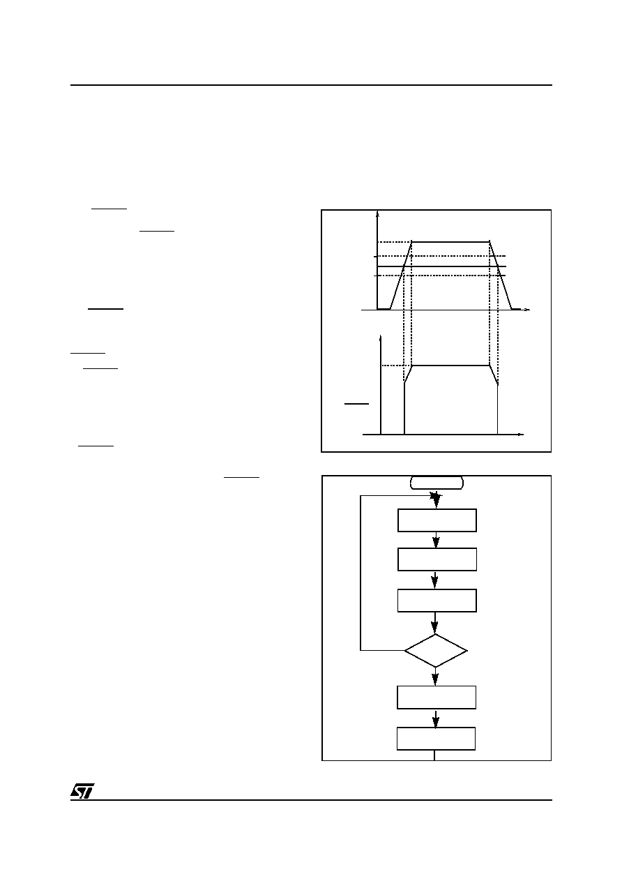
The internal POR device is a static mechanism
which forces the reset state when VDD is below a
threshold voltage in the range 3.4 to 4.2 Volts (see
Figure 13). The circuit guarantees that the MCU
will exit or enter the reset state correctly, without
spurious effects, ensuring, for example, that EEP-
ROM contents are not corrupted.
Note: This feature is not available on OTP/EPROM
Devices.
Figure 13. Power ON/OFF Reset operation
Figure 14. Reset and Interrupt Processing
VR02037
VDD
4.2
3.4
t
V
t
POWER
ON/OFF
Threshold
DD
RESET
INT LATCH CLEARED
NMI MASK SET
RESET
( IF PRESENT )
SELECT
NMI MODE FLAGS
IS RESET STILL
PRESENT?
YES
PUT FFEH
ON ADDRESS BUS
FROM RESET LOCATIONS
FFE/FFF
NO
FETCH INSTRUCTION
LOAD PC
VA000427
相關(guān)PDF資料 |
PDF描述 |
|---|---|
| ST6382B1/XXX | 8-BIT, MROM, MICROCONTROLLER, PDIP42 |
| ST6386B1 | 8-BIT, MROM, 8 MHz, MICROCONTROLLER, PDIP42 |
| ST6388B1 | 8-BIT, MROM, 8 MHz, MICROCONTROLLER, PDIP42 |
| ST6387B1 | 8-BIT, MROM, 8 MHz, MICROCONTROLLER, PDIP42 |
| ST6394B1 | 8-BIT, MROM, 8 MHz, MICROCONTROLLER, PDIP42 |
相關(guān)代理商/技術(shù)參數(shù) |
參數(shù)描述 |
|---|---|
| ST6369 | 制造商:STMICROELECTRONICS 制造商全稱:STMicroelectronics 功能描述:8-BIT HCMOS MCU FOR DIGITAL CONTROLLED MULTI FREQUENCYMONITOR |
| ST6369B1 | 制造商:未知廠家 制造商全稱:未知廠家 功能描述:Microcontroller |
| ST6-36B28 | 功能描述:電源變壓器 SPLIT BOBBIN HORZ MOUNT XFMR RoHS:否 制造商:Triad Magnetics 功率額定值:12 VA 初級電壓額定值:115 V / 230 V 次級電壓額定值:12 V / 24 V 安裝風(fēng)格:SMD/SMT 一次繞組:Dual Primary Winding 二次繞組:Dual Secondary Winding 長度:2.5 in 寬度:2 in 高度:1.062 in |
| ST6371 | 制造商:未知廠家 制造商全稱:未知廠家 功能描述:Microcontroller |
| ST6372 | 制造商:未知廠家 制造商全稱:未知廠家 功能描述:Microcontroller |
發(fā)布緊急采購,3分鐘左右您將得到回復(fù)。