- 您現(xiàn)在的位置:買賣IC網(wǎng) > PDF目錄361344 > T436416D-5C (TM Technology, Inc.) 4M x 16 SDRAM 1M x 16bit x 4Banks Synchronous DRAM PDF資料下載
參數(shù)資料
| 型號(hào): | T436416D-5C |
| 廠商: | TM Technology, Inc. |
| 英文描述: | 4M x 16 SDRAM 1M x 16bit x 4Banks Synchronous DRAM |
| 中文描述: | 4米× 16 SDRAM的100萬(wàn)x 16Bit的X 4Banks同步DRAM |
| 文件頁(yè)數(shù): | 6/73頁(yè) |
| 文件大小: | 734K |
| 代理商: | T436416D-5C |
第1頁(yè)第2頁(yè)第3頁(yè)第4頁(yè)第5頁(yè)當(dāng)前第6頁(yè)第7頁(yè)第8頁(yè)第9頁(yè)第10頁(yè)第11頁(yè)第12頁(yè)第13頁(yè)第14頁(yè)第15頁(yè)第16頁(yè)第17頁(yè)第18頁(yè)第19頁(yè)第20頁(yè)第21頁(yè)第22頁(yè)第23頁(yè)第24頁(yè)第25頁(yè)第26頁(yè)第27頁(yè)第28頁(yè)第29頁(yè)第30頁(yè)第31頁(yè)第32頁(yè)第33頁(yè)第34頁(yè)第35頁(yè)第36頁(yè)第37頁(yè)第38頁(yè)第39頁(yè)第40頁(yè)第41頁(yè)第42頁(yè)第43頁(yè)第44頁(yè)第45頁(yè)第46頁(yè)第47頁(yè)第48頁(yè)第49頁(yè)第50頁(yè)第51頁(yè)第52頁(yè)第53頁(yè)第54頁(yè)第55頁(yè)第56頁(yè)第57頁(yè)第58頁(yè)第59頁(yè)第60頁(yè)第61頁(yè)第62頁(yè)第63頁(yè)第64頁(yè)第65頁(yè)第66頁(yè)第67頁(yè)第68頁(yè)第69頁(yè)第70頁(yè)第71頁(yè)第72頁(yè)第73頁(yè)

TE
CH
tm
Commands
T436416D
TM Technology Inc. reserves the right
P. 6
to change products or specifications without notice.
Publication Date: FEB. 2007
Revision: A
1
BankActivate
(RAS# = "L", CAS# = "H", WE# = "H", BAs = Bank, A0-A11 = Row Address)
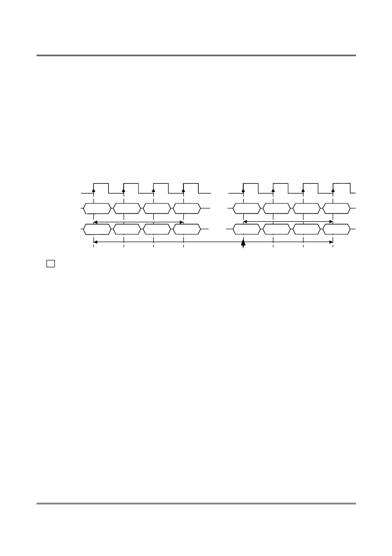
The BankActivate command activates the idle bank designated by the BA0,1 signals. By latching the row
address on A0 to A11 at the time of this command, the selected row access is initiated. The read or write
operation in the same bank can occur after a time delay of t
RCD
(min.) from the time of bank activation. A
subsequent BankActivate command to a different row in the same bank can only be issued after the previous
active row has been precharged (refer to the following figure). The minimum time interval between successive
BankActivate commands to the same bank is defined by t
RC
(min.). The SDRAM has four internal banks on the
same chip and shares part of the internal circuitry to reduce chip area; therefore it restricts the back-to-back
activation of the four banks. t
RRD
(min.) specifies the minimum time required between activating different banks.
After this command is used, the Write command and the Block Write command perform the no mask write
operation.
CLK
ADDRESS
T0
T 1
T2
T3
Tn+3
Tn+4
Tn+5
Tn+6
..............
COMMAND
..............
..............
NOP
NOP
NOP
NOP
RAS# - CAS# delay (
t
RCD
)
RAS# - RAS# delay time (
t
RRD
)
RAS# Cycle time (
t
RC
)
Bank A
Row Addr.
Bank A
Col Addr.
Bank B
Row Addr.
Bank A
Row Addr.
Bank A
Activate
R/W A with
AutoPrecharge
Bank B
Activate
Bank A
Activate
AutoPrecharge
Begin
: "H" or "L"
BankActivate Command Cycle
(Burst Length = n, CAS# Latency = 3)
2
BankPrecharge command
(RAS# = "L", CAS# = "H", WE# = "L", BAs = Bank, A10 = "L", A0-A9 and A11 = Don't care)
The BankPrecharge command precharges the bank designated by BA signal. The precharged bank is
switched from the active state to the idle state. This command can be asserted anytime after t
RAS
(min.) is
satisfied from the BankActivate command in the desired bank. The maximum time any bank can be active is
specified by t
RAS
(max.). Therefore, the precharge function must be performed in any active bank within
t
RAS
(max.). At the end of precharge, the precharged bank is still in the idle state and is ready to be activated
again.
3
PrechargeAll command
(RAS# = "L", CAS# = "H", WE# = "L", BAs = Don’t care, A10 = "H", A0-A9 and A11 = Don't care)
The PrechargeAll command precharges all banks simultaneously and can be issued even if all banks are
not in the active state. All banks are then switched to the idle state.
4
Read command
(RAS# = "H", CAS# = "L", WE# = "H", BAs = Bank, A10 = "L", A0-A7 = Column Address)
The Read command is used to read a burst of data on consecutive clock cycles from an active row in an
active bank. The bank must be active for at least t
RCD
(min.) before the Read command is issued. During read
bursts, the valid data-out element from the starting column address will be available following the CAS#
latency after the issue of the Read command. Each subsequent data-out element will be valid by the next
positive clock edge (refer to the following figure). The DQs go into high-impedance at the end of the burst
unless other command is initiated. The burst length, burst sequence, and CAS# latency are determined by the
mode register, which is already programmed. A full-page burst will continue until terminated (at the end of the
page it will wrap to column 0 and continue).
相關(guān)PDF資料 |
PDF描述 |
|---|---|
| T436416D-5CG | 4M x 16 SDRAM 1M x 16bit x 4Banks Synchronous DRAM |
| T436416D-5S | 4M x 16 SDRAM 1M x 16bit x 4Banks Synchronous DRAM |
| T436416D-5SG | 4M x 16 SDRAM 1M x 16bit x 4Banks Synchronous DRAM |
| T436416D-6C | 4M x 16 SDRAM 1M x 16bit x 4Banks Synchronous DRAM |
| T436416D-6CG | 4M x 16 SDRAM 1M x 16bit x 4Banks Synchronous DRAM |
相關(guān)代理商/技術(shù)參數(shù) |
參數(shù)描述 |
|---|---|
| T436416D-5CG | 制造商:TMT 制造商全稱:TMT 功能描述:4M x 16 SDRAM 1M x 16bit x 4Banks Synchronous DRAM |
| T436416D-5S | 制造商:TMT 制造商全稱:TMT 功能描述:4M x 16 SDRAM 1M x 16bit x 4Banks Synchronous DRAM |
| T436416D-5SG | 制造商:TMT 制造商全稱:TMT 功能描述:4M x 16 SDRAM 1M x 16bit x 4Banks Synchronous DRAM |
| T436416D-6C | 制造商:TMT 制造商全稱:TMT 功能描述:4M x 16 SDRAM 1M x 16bit x 4Banks Synchronous DRAM |
| T436416D-6CG | 制造商:TMT 制造商全稱:TMT 功能描述:4M x 16 SDRAM 1M x 16bit x 4Banks Synchronous DRAM |
發(fā)布緊急采購(gòu),3分鐘左右您將得到回復(fù)。