- 您現(xiàn)在的位置:買(mǎi)賣(mài)IC網(wǎng) > PDF目錄98158 > TAS3202PAG (TEXAS INSTRUMENTS INC) SPECIALTY CONSUMER CIRCUIT, PQFP64 PDF資料下載
參數(shù)資料
| 型號(hào): | TAS3202PAG |
| 廠商: | TEXAS INSTRUMENTS INC |
| 元件分類(lèi): | 消費(fèi)家電 |
| 英文描述: | SPECIALTY CONSUMER CIRCUIT, PQFP64 |
| 封裝: | GREEN, PLASTIC, TQFP-64 |
| 文件頁(yè)數(shù): | 44/66頁(yè) |
| 文件大?。?/td> | 817K |
| 代理商: | TAS3202PAG |
第1頁(yè)第2頁(yè)第3頁(yè)第4頁(yè)第5頁(yè)第6頁(yè)第7頁(yè)第8頁(yè)第9頁(yè)第10頁(yè)第11頁(yè)第12頁(yè)第13頁(yè)第14頁(yè)第15頁(yè)第16頁(yè)第17頁(yè)第18頁(yè)第19頁(yè)第20頁(yè)第21頁(yè)第22頁(yè)第23頁(yè)第24頁(yè)第25頁(yè)第26頁(yè)第27頁(yè)第28頁(yè)第29頁(yè)第30頁(yè)第31頁(yè)第32頁(yè)第33頁(yè)第34頁(yè)第35頁(yè)第36頁(yè)第37頁(yè)第38頁(yè)第39頁(yè)第40頁(yè)第41頁(yè)第42頁(yè)第43頁(yè)當(dāng)前第44頁(yè)第45頁(yè)第46頁(yè)第47頁(yè)第48頁(yè)第49頁(yè)第50頁(yè)第51頁(yè)第52頁(yè)第53頁(yè)第54頁(yè)第55頁(yè)第56頁(yè)第57頁(yè)第58頁(yè)第59頁(yè)第60頁(yè)第61頁(yè)第62頁(yè)第63頁(yè)第64頁(yè)第65頁(yè)第66頁(yè)
www.ti.com
SLES208B – JUNE 2009 – REVISED MARCH 2011
9.3
I
2C Memory Load Control and Memory Load Data Registers (0x04 and 0x05)
Registers 0x04 (Table 9-4) and 0x05 (Table 9-5) allow the user to download TAS3202 program code and
data directly from the system I2C controller. This mode is called the I2C slave mode (from the TAS3202
point of view). See the TAS3xxx Firmware Programmer's Guide for more details.
The I2C slave memory load port permits the system controller to load the TAS3202 memories as an
alternative to having the TAS3202 load its memory from EEPROM.
Micro program memory
Micro extended memory
DAP program memory
DAP coefficient memory
DAP data memory
The transfer is performed by writing to two I2C registers. The first register is an 8-byte register that holds
the checksum, the memory to be written, the starting address, the number of data bytes to be transferred.
The second location holds 8 bytes of data. The memory load operation starts with the first register being
set. Then the data is written into the second register using the format shown. After the last data byte is
written into the second register, an additional two bytes are written that contain the 2-byte checksum. At
that point, the transfer is complete and status of the operation is reported in the status register. The end
checksum is always contained in the last two bytes of the data block.
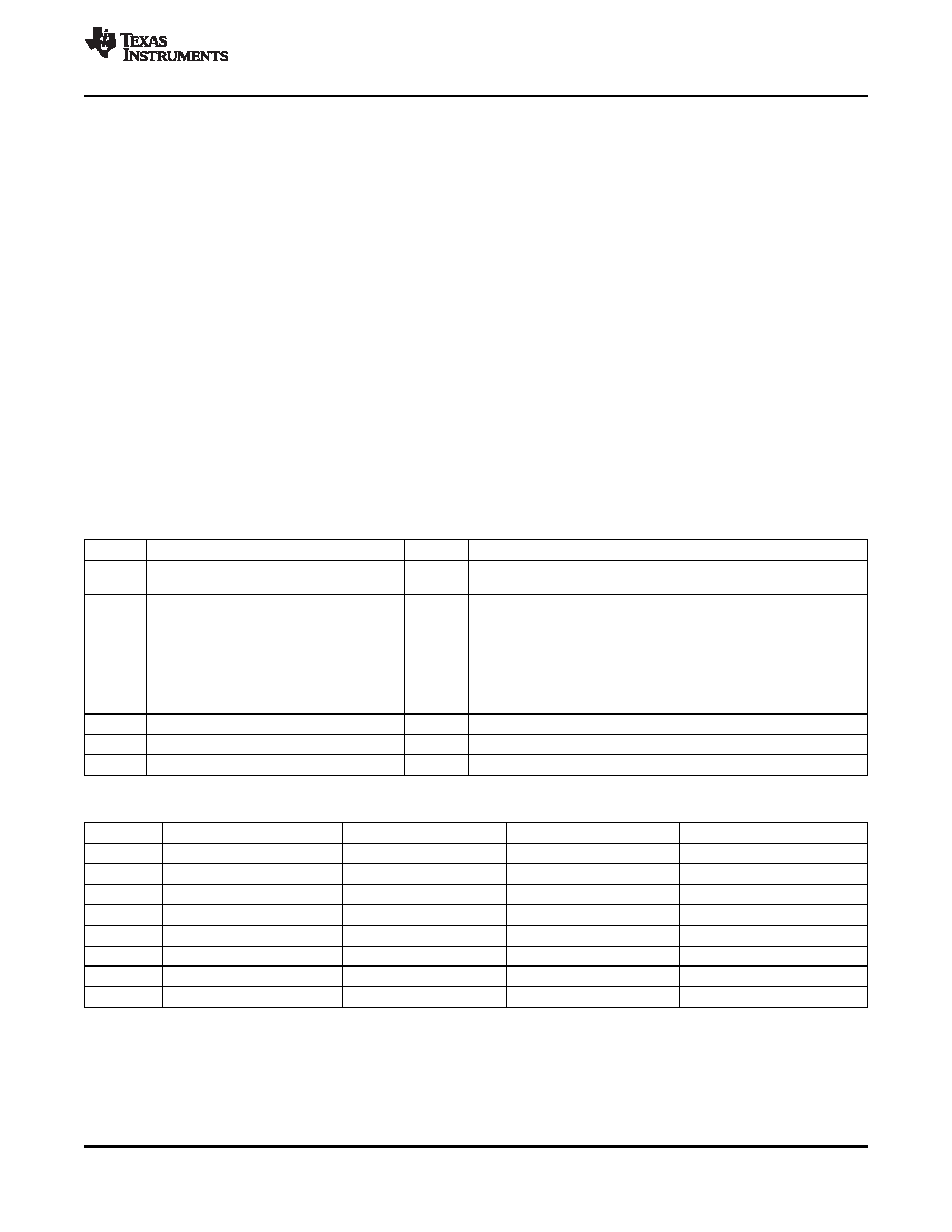
Table 9-4. TAS3202 Memory Load Control Register (0x04)
BYTE
DATA BLOCK FORMAT
SIZE
NOTES
Checksum of bytes 2 through N + 8. If this is a termination header,
1–2
Checksum code
2 bytes
this value is 00 00.
0: Microprocessor program memory
1: Microprocessor external data memory
2: Audio DSP core program memory
3: Audio DSP core coefficient memory
3-4
Memory to be loaded
2 bytes
4: Audio DSP core data memory
5: Audio DSP core upper data memory
6: Audio DSP core upper coefficient memory
7–15: Reserved for future expansion
5
Unused
1 byte
Reserved for future expansion
6–7
Starting TAS3202 memory address
2 bytes
If this is a termination header, this value is 0000.
7–8
Number of data bytes to be transferred
2 bytes
If this is a termination header, this value is 0000.
Table 9-5. TAS3202 Memory Load Data Register (0x05)
BYTE
8-BIT DATA
28-BIT DATA
48-BIT DATA
54-BIT DATA
1
Datum 1 D7–D0
0000 D27–D24
0000 0000
2
Datum 2 D7–D0
D7–D0
0000 0000
00 D53–D48
3
Datum 3 D7–D0
D15–D8
D47–D40
4
Datum 4 D7–D0
D7–D0
D39–D32
5
Datum 5 D7–D0
0000 D27–D24
D31–D24
6
Datum 6 D7–D0
D23–D16
7
Datum 7 D7–D0
D15–D8
8
Datum 8 D7–D0
D7–D0
Copyright 2009–2011, Texas Instruments Incorporated
49
I2C Register Map
Product Folder Link(s): TAS3202
相關(guān)PDF資料 |
PDF描述 |
|---|---|
| TAS3204PAGR | SPECIALTY CONSUMER CIRCUIT, PQFP64 |
| TAS3204PAG | SPECIALTY CONSUMER CIRCUIT, PQFP64 |
| TAS3218IPZPR | SPECIALTY CONSUMER CIRCUIT, PQFP100 |
| TAS3218IPZP | SPECIALTY CONSUMER CIRCUIT, PQFP100 |
| TAS3218PZPR | SPECIALTY CONSUMER CIRCUIT, PQFP100 |
相關(guān)代理商/技術(shù)參數(shù) |
參數(shù)描述 |
|---|---|
| TAS3202PAGR | 功能描述:音頻 DSP Hi Perf Dig Aud SOC RoHS:否 制造商:Texas Instruments 工作電源電壓: 電源電流: 工作溫度范圍: 安裝風(fēng)格: 封裝 / 箱體: 封裝:Tube |
| TAS3204 | 制造商:TI 制造商全稱(chēng):Texas Instruments 功能描述:AUDIO DSP WITH ANALOG INTERFACE |
| TAS3204EVM | 功能描述:音頻 IC 開(kāi)發(fā)工具 TAS3204EVM Eval Mod RoHS:否 制造商:Texas Instruments 產(chǎn)品:Evaluation Kits 類(lèi)型:Audio Amplifiers 工具用于評(píng)估:TAS5614L 工作電源電壓:12 V to 38 V |
| TAS3204EVM-LC | 制造商:Texas Instruments 功能描述:TAS3204EVM EVALUATION MODULE - Boxed Product (Development Kits) |
| TAS3204PAG | 功能描述:音頻 DSP Hi Perf Dual Core DSP/MCU Aud Proc RoHS:否 制造商:Texas Instruments 工作電源電壓: 電源電流: 工作溫度范圍: 安裝風(fēng)格: 封裝 / 箱體: 封裝:Tube |
發(fā)布緊急采購(gòu),3分鐘左右您將得到回復(fù)。