- 您現(xiàn)在的位置:買賣IC網(wǎng) > PDF目錄98163 > TAS5424ATPHDQ1 (TEXAS INSTRUMENTS INC) 116 W, 4 CHANNEL, AUDIO AMPLIFIER, PQFP64 PDF資料下載
參數(shù)資料
| 型號: | TAS5424ATPHDQ1 |
| 廠商: | TEXAS INSTRUMENTS INC |
| 元件分類: | 音頻/視頻放大 |
| 英文描述: | 116 W, 4 CHANNEL, AUDIO AMPLIFIER, PQFP64 |
| 封裝: | PLASTIC, HTQFP-64 |
| 文件頁數(shù): | 13/51頁 |
| 文件大?。?/td> | 1422K |
| 代理商: | TAS5424ATPHDQ1 |
第1頁第2頁第3頁第4頁第5頁第6頁第7頁第8頁第9頁第10頁第11頁第12頁當(dāng)前第13頁第14頁第15頁第16頁第17頁第18頁第19頁第20頁第21頁第22頁第23頁第24頁第25頁第26頁第27頁第28頁第29頁第30頁第31頁第32頁第33頁第34頁第35頁第36頁第37頁第38頁第39頁第40頁第41頁第42頁第43頁第44頁第45頁第46頁第47頁第48頁第49頁第50頁第51頁

50V
100ms
Max
MaxRampRate
15V/ms
PVDD
50V
29V
26V
23V
22V
14.4V
Hi-Z AllCh’s
I CStop
StandbyMode
2
LoadDumpProtection
29V–50V
OvervoltageProtectionRegion
23V–29V
NormalOperatingRegion
8V–22V
Time
POR
I CStart
2
ReadytoGet
OffHi-ZState
T0189-01
SLOS535B – MAY 2009 – REVISED JANUARY 2010
www.ti.com
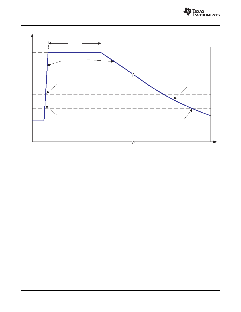
Figure 15. Voltage Operating Regions With Load Dump Transition Defined
Power Supply
The power for the device is most commonly provided by a car battery that can have a large voltage swing, 8 Vdc
to 18 Vdc. PVDD is a filtered battery voltage, and it is the supply for the output FETS and the low-side FET gate
driver. The high-side FET gate driver is supplied by a charge pump (CP) supply. The charge pump supplies the
gate drive voltage for all four channels. The analog circuitry is powered by AVDD, which is a provided by an
internal linear regulator. A 0.1mF/10V external bypass capacitor is needed at the A_BYP pin for this supply. It is
recommended that no external components except the bypass capacitor be attached to this pin. The digital
circuitry is powered by DVDD, which is provided by an internal linear regulator. A 0.1mF/10V external bypass
capacitor is needed at the D_BYP pin. It is recommended that no external components except the bypass
capacitor be attached to this pin.
The TAS5414A and TAS5424A can withstand fortuitous open ground and power conditions. Fortuitous open
ground usually occurs when a speaker wire is shorted to ground, allowing for a second ground path through the
body diode in the output FETs. The uniqueness of the diagnostic capabilities allows the speakers and speaker
wires to be debugged, eliminating the need to remove the amplifier to diagnose the problem.
I
2C Serial Communication Bus
The TAS5414A and TAS5424A communicate with the system processor via the I2C serial communication bus.
The TAS5414A and TAS5424A are I2C slave-only devices. The processor can poll the TAS5414A and the
TAS5424A via I2C to determine the operating status of the device. All fault conditions and detections are
reported via I2C. There are also numerous features and operating conditions that can be set via I2C.
The I2C bus allows control of the following configurations:
Independent gain control of each channel. The gain can be set to 12 dB, 20 dB, 26 dB, and 32 dB.
Select current limit (for 2-
and for 4- loads). This allows optimal design of the filter inductor, and the use of
smaller gauge speaker wires for 4-
applications.
20
Copyright 2009–2010, Texas Instruments Incorporated
相關(guān)PDF資料 |
PDF描述 |
|---|---|
| TAS5424ATPHDRMQ1 | 116 W, 4 CHANNEL, AUDIO AMPLIFIER, PQFP64 |
| TAS5424ATPHDRQ1 | 116 W, 4 CHANNEL, AUDIO AMPLIFIER, PQFP64 |
| TAS5424TDKDQ1 | 116 W, 4 CHANNEL, AUDIO AMPLIFIER, PDSO44 |
| TAS5424TDKDRQ1 | 116 W, 4 CHANNEL, AUDIO AMPLIFIER, PDSO44 |
| TAS5424TDKDQ1G4 | 116 W, 4 CHANNEL, AUDIO AMPLIFIER, PDSO44 |
相關(guān)代理商/技術(shù)參數(shù) |
參數(shù)描述 |
|---|---|
| TAS5424ATPHDRMQ1 | 制造商:TI 制造商全稱:Texas Instruments 功能描述:FOUR-CHANNEL AUTOMOTIVE DIGITAL AMPLIFIERS |
| TAS5424ATPHDRQ1 | 制造商:TI 制造商全稱:Texas Instruments 功能描述:FOUR-CHANNEL AUTOMOTIVE DIGITAL AMPLIFIERS |
| TAS5424BQ1DKDEVM | 功能描述:音頻 IC 開發(fā)工具 TAS5424BQ1DKD EVAL MOD RoHS:否 制造商:Texas Instruments 產(chǎn)品:Evaluation Kits 類型:Audio Amplifiers 工具用于評估:TAS5614L 工作電源電壓:12 V to 38 V |
| TAS5424BTDKDQ1 | 制造商:Texas Instruments 功能描述:- Trays |
| TAS5424BTDKDRQ1 | 功能描述:音頻放大器 Four-CH Auto Digital Amps RoHS:否 制造商:STMicroelectronics 產(chǎn)品:General Purpose Audio Amplifiers 輸出類型:Digital 輸出功率: THD + 噪聲: 工作電源電壓:3.3 V 電源電流: 最大功率耗散: 最大工作溫度: 安裝風(fēng)格:SMD/SMT 封裝 / 箱體:TQFP-64 封裝:Reel |
發(fā)布緊急采購,3分鐘左右您將得到回復(fù)。