- 您現(xiàn)在的位置:買賣IC網(wǎng) > PDF目錄299957 > TC1017-2.6VCTTR 2.6 V FIXED POSITIVE LDO REGULATOR, 0.5 V DROPOUT, PDSO5 PDF資料下載
參數(shù)資料
| 型號: | TC1017-2.6VCTTR |
| 元件分類: | 固定正電壓單路輸出LDO穩(wěn)壓器 |
| 英文描述: | 2.6 V FIXED POSITIVE LDO REGULATOR, 0.5 V DROPOUT, PDSO5 |
| 封裝: | PLASTIC, MO-178, SOT-23, 5 PIN |
| 文件頁數(shù): | 12/22頁 |
| 文件大?。?/td> | 357K |
| 代理商: | TC1017-2.6VCTTR |
TC1017
DS21813D-page 2
2005 Microchip Technology Inc.
1.0
ELECTRICAL
CHARACTERISTICS
Absolute Maximum Ratings
Input Voltage ....................................................................6.5V
Power Dissipation ......................... Internally Limited (Note 7)
Maximum Voltage On Any Pin ..................VIN + 0.3V to -0.3V
Notice: Stresses above those listed under "Maximum
Ratings" may cause permanent damage to the device. This is
a stress rating only and functional operation of the device at
those or any other conditions above those indicated in the
operation listings of this specification is not implied. Exposure
to maximum rating conditions for extended periods may affect
device reliability.
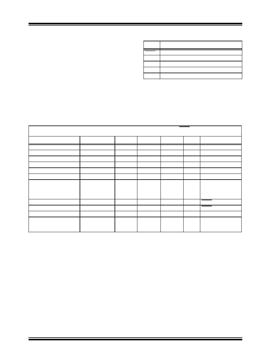
PIN FUNCTION TABLE
Name
Function
SHDN
Shutdown control input.
NC
No connect
GND
Ground terminal
VOUT
Regulated voltage output
VIN
Unregulated supply input
ELECTRICAL CHARACTERISTICS
Electrical Specifications: Unless otherwise noted, VIN = VR + 1V, IL = 100 A, CL = 1.0 F, SHDN > VIH, TA = +25°C
Boldface type specifications apply for junction temperatures of –40°C to +125°C.
Parameter
Sym
Min
Typ
Max
Units
Test Conditions
Input Operating Voltage
VIN
2.7
—
6.0
V
Maximum Output Current
IOUTMAX
150
——
mA
Output Voltage
VOUT
VR – 2.5%
VR ±0.5%
VR + 2.5%
V
V
OUT Temperature Coefficient
TCVOUT
—
40
—
ppm/°C
Line Regulation
|(ΔVOUT/ΔVIN)| / V
R
—0.04
0.2
%/V
(VR + 1V) < VIN < 6V
Load Regulation (Note 4)
|ΔVOUT| / VR
—0.38
1.5
%IL = 0.1 mA to IOUTMAX
Dropout Voltage (Note 5)
VIN – VOUT
—
2
90
180
285
—
200
350
500
mV
IL = 100 A
IL = 50 mA
IL = 100 mA
IL = 150 mA
Supply Current
IIN
—53
90
A
SHDN = VIH, IL = 0
Shutdown Supply Current
IINSD
—
0.05
2
A
SHDN = 0V
Power Supply Rejection Ratio
PSRR
—
58
—
dB
f =1 kHz, IL = 50 mA
Wake-Up Time
(from Shutdown Mode)
tWK
—10
—
s
VIN = 5V, IL = 60 mA,
CIN = COUT =1 F,
f = 100 Hz
Note
1:
The minimum V
IN has to meet two conditions: VIN ≥ 2.7V and VIN ≥ (VR + 2.5%) + VDROPOUT.
2:
V
R is the regulator voltage setting. For example: VR = 1.8V, 2.7V, 2.8V, 3.0V.
3:
4:
Regulation is measured at a constant junction temperature using low duty-cycle pulse testing. Load regulation is tested
over a load range from 0.1 mA to the maximum specified output current. Changes in output voltage due to heating
effects are covered by the thermal regulation specification.
5:
Dropout voltage is defined as the input-to-output differential at which the output voltage drops 2% below its nominal
value at a 1V differential.
6:
Thermal regulation is defined as the change in output voltage at a time T after a change in power dissipation is applied,
excluding load or line regulation effects. Specifications are for a current pulse equal to ILMAX at VIN = 6V for t = 10 msec.
7:
The maximum allowable power dissipation is a function of ambient temperature, the maximum allowable junction
temperature and the thermal resistance from junction-to-air (i.e., T
A, TJ, θJA). Exceeding the maximum allowable power
dissipation causes the device to initiate thermal shutdown. Please see Section 5.1 “Thermal Shutdown”, for more
details
.
8:
Output current is limited to 120 mA (typ) when V
OUT is less than 0.5V due to a load fault or short-circuit condition.
TCV
OUT
V
OUTMAX
V
OUTMIN
–
() 10
6
×
V
OUT
T
Δ
×
--------------------------------------------------------------------------------------
=
相關(guān)PDF資料 |
PDF描述 |
|---|---|
| TC105550ECT | 5 V FIXED POSITIVE LDO REGULATOR, 0.25 V DROPOUT, PDSO5 |
| TC105550ECT723 | 5 V FIXED POSITIVE LDO REGULATOR, 0.25 V DROPOUT, PDSO5 |
| TC1301A-NICVMFTR | DUAL OUTPUT, FIXED POSITIVE LDO REGULATOR, PDSO8 |
| TC1301B-FFAVMFTR | DUAL OUTPUT, FIXED POSITIVE LDO REGULATOR, PDSO8 |
| TC1N5224B.TR | 2.8 V, 0.5 W, SILICON, UNIDIRECTIONAL VOLTAGE REGULATOR DIODE, DO-35 |
相關(guān)代理商/技術(shù)參數(shù) |
參數(shù)描述 |
|---|---|
| TC1017-3.0VCT | 制造商:MICROCHIP 制造商全稱:Microchip Technology 功能描述:150 mA, Tiny CMOS LDO With Shutdown |
| TC1017-3.0VCTTR | 功能描述:低壓差穩(wěn)壓器 - LDO 150mA CMOS LDO RoHS:否 制造商:Texas Instruments 最大輸入電壓:36 V 輸出電壓:1.4 V to 20.5 V 回動電壓(最大值):307 mV 輸出電流:1 A 負載調(diào)節(jié):0.3 % 輸出端數(shù)量: 輸出類型:Fixed 最大工作溫度:+ 125 C 安裝風格:SMD/SMT 封裝 / 箱體:VQFN-20 |
| TC1017-3.0VLT | 制造商:MICROCHIP 制造商全稱:Microchip Technology 功能描述:150 mA, Tiny CMOS LDO With Shutdown |
| TC1017-3.0VLTTR | 功能描述:低壓差穩(wěn)壓器 - LDO 150mA Adj LDO RoHS:否 制造商:Texas Instruments 最大輸入電壓:36 V 輸出電壓:1.4 V to 20.5 V 回動電壓(最大值):307 mV 輸出電流:1 A 負載調(diào)節(jié):0.3 % 輸出端數(shù)量: 輸出類型:Fixed 最大工作溫度:+ 125 C 安裝風格:SMD/SMT 封裝 / 箱體:VQFN-20 |
| TC1017-3.3VCT | 制造商:MICROCHIP 制造商全稱:Microchip Technology 功能描述:150 mA, Tiny CMOS LDO With Shutdown |
發(fā)布緊急采購,3分鐘左右您將得到回復(fù)。