- 您現在的位置:買賣IC網 > PDF目錄98171 > TC655EUN BRUSHLESS DC MOTOR CONTROLLER, PDSO10 PDF資料下載
參數資料
| 型號: | TC655EUN |
| 元件分類: | 運動控制電子 |
| 英文描述: | BRUSHLESS DC MOTOR CONTROLLER, PDSO10 |
| 封裝: | PLASTIC, MSOP-10 |
| 文件頁數: | 8/36頁 |
| 文件大小: | 706K |
| 代理商: | TC655EUN |
第1頁第2頁第3頁第4頁第5頁第6頁第7頁當前第8頁第9頁第10頁第11頁第12頁第13頁第14頁第15頁第16頁第17頁第18頁第19頁第20頁第21頁第22頁第23頁第24頁第25頁第26頁第27頁第28頁第29頁第30頁第31頁第32頁第33頁第34頁第35頁第36頁

TC654/TC655
DS21734A-page 16
2002 Microchip Technology Inc.
The data on the line must be changed during the LOW
period of the clock signal. There is one clock pulse per
bit of data. Each data transfer is initiated with a START
condition and terminated with a STOP condition. The
number of the data bytes transferred between the
START and STOP conditions is determined by the
master device and is unlimited.
5.1.7
ACKNOWLEDGE (ACK)
Each receiving device, when addressed, is obliged to
generate an acknowledge bit after the reception of
each byte. The master device must generate an extra
clock pulse, which is associated with this acknowledge
bit.
The device that acknowledges has to pull down the
SDA line during the acknowledge clock pulse in such a
way that the SDA line is stable LOW during the HIGH
period of the acknowledge related clock pulse. Setup
and hold times must be taken into account. During
reads, a master device must signal an end of data to
the slave by not generating an acknowledge bit on the
last byte that has been clocked out of the slave. In this
case, the slave (TC654/TC655) will leave the data line
HIGH to enable the master device to generate the
STOP condition.
5.2
SMBus Protocols
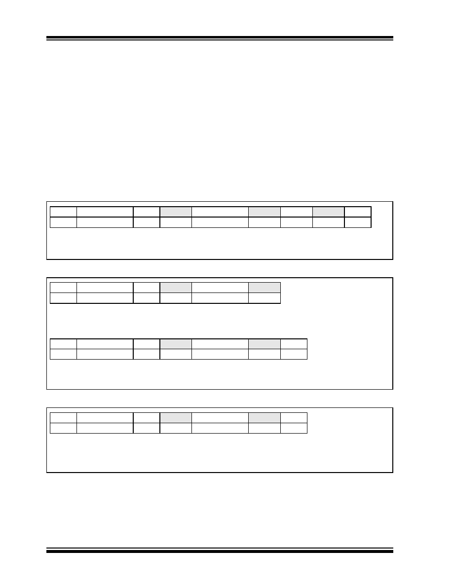
The TC654/TC655 devices communicate with three
standard SMBus protocols. These are the write byte,
read byte and receive byte. The receive byte is a short-
ened method for reading from, or writing to, a register
which had been selected by the previous read or write
command. These transmission protocols are shown in
FIGURE 5-1:
SMBus Protocol: Write Byte Format.
FIGURE 5-2:
SMBus Protocol: Read Byte Format.
FIGURE 5-3:
SMBus Protocol: Receive Byte Format.
S
ADDRESS
WR
ACK
COMMAND
ACK
DATA
ACK
P
7 Bits
8 Bits
Slave Address
Command Byte: selects
which register you are
writing to.
Data Byte: data goes
into the register set
by the command byte.
S
ADDRESS
WR
ACK
COMMAND
ACK
7 Bits
8 Bits
Slave Address
Command Byte: selects
which register you are
writing to.
S
ADDRESS
RD
ACK
DATA
NACK
P
7 Bits
8 Bits
Slave Address:
repeated due to change
in data flow direction.
Data Byte: reads from
the register set by the
command byte.
S
ADDRESS
RD
ACK
DATA
NACK
P
7 Bits
8 Bits
Slave Address
Data Byte: reads data from
the register commanded by
the last Read Byte or Write
Byte transmission
S = Start Condition
P = Stop Condition
Shaded = Slave Transmission
ACK = Acknowledge = 0
NACK = Not Acknowledged = 1
WR = Write = 0
RD = Read = 1
相關PDF資料 |
PDF描述 |
|---|---|
| TC654EUNTR | BRUSHLESS DC MOTOR CONTROLLER, PDSO10 |
| TC665EUN | BRUSHLESS DC MOTOR CONTROLLER, PDSO10 |
| TC7106ARCPLIJL | 1-CH DUAL-SLOPE ADC, ACCESS, PDIP40 |
| TC7106CPLIJL | 1-CH DUAL-SLOPE ADC, ACCESS, PDIP40 |
| TC7107ARCPLIJL | 1-CH DUAL-SLOPE ADC, ACCESS, PDIP40 |
相關代理商/技術參數 |
參數描述 |
|---|---|
| TC655EUNTR | 功能描述:軟開關 PWM 控制器 Dual RoHS:否 制造商:Fairchild Semiconductor 輸出端數量: 輸出電流: 開關頻率: 工作電源電壓:30 V 電源電流: 最大工作溫度:+ 105 C 最小工作溫度:- 40 C 安裝風格:SMD/SMT 封裝 / 箱體:SOIC-8 封裝:Reel |
| TC65A | 制造商:CDE 制造商全稱:Cornell Dubilier Electronics 功能描述:Axial Leaded Aluminum Electrolytic Capacitors |
| TC65I | 制造商:CINTERION 功能描述:MODULE GSM/GPRS QUADBAND + JAVA TC65I 制造商:CINTERION 功能描述:MOD, GSM / GPRS, QUAD BAND, TCP/IP 制造商:CINTERION 功能描述:MOD, GSM / GPRS, QUAD BAND, I2C, SPI, USB, TCP/IP; No. of Channels:4; Supply Voltage Min:3.2V; Supply Voltage Max:4.5V; Frequency RF:1900MHz; Module Interface:I2C, SPI, USB; RF Coax Type:1.9 GHz; Supply Voltage Range:3.2V to 4.5V ;RoHS Compliant: Yes |
| TC65I L30960-N1150-A100 | 制造商:Gemalto 功能描述: |
| TC65I X GPIO TERMINAL | 制造商:MC TECHNOLOGIES 功能描述:MOD QUADBAND GPIO JAVA TERMIN 制造商:MC TECHNOLOGIES 功能描述:MOD, QUADBAND GPIO JAVA TERMINAL 制造商:MC TECHNOLOGIES 功能描述:MOD, QUADBAND GPIO JAVA TERMINAL; No. of Channels:4; Protocol:TCP / IP; Supply Voltage Min:8V; Supply Voltage Max:30V; Frequency RF:1.9GHz; Module Interface:RS232; Kit Features:GPRS upto 86kbps, Data CSD upto 14.4kbps, Secure Data ;RoHS Compliant: Yes |
發(fā)布緊急采購,3分鐘左右您將得到回復。