- 您現(xiàn)在的位置:買賣IC網(wǎng) > PDF目錄361408 > TC7107CPL (TelCom Semiconductor, Inc.) 3-1/2 DIGIT A/D CONVERTERS PDF資料下載
參數(shù)資料
| 型號(hào): | TC7107CPL |
| 廠商: | TelCom Semiconductor, Inc. |
| 元件分類: | 串行ADC |
| 英文描述: | 3-1/2 DIGIT A/D CONVERTERS |
| 中文描述: | 3-1/2位數(shù)的A / D轉(zhuǎn)換器 |
| 文件頁數(shù): | 7/19頁 |
| 文件大?。?/td> | 296K |
| 代理商: | TC7107CPL |

3-189
TELCOM SEMICONDUCTOR, INC.
7
6
5
4
3
1
2
8
The dual slope converter accuracy is unrelated to the
integrating resistor and capacitor values as long as they are
stable during a measurement cycle. An inherent benefit is
noise immunity. Noise spikes are integrated or averaged to
zero during the integration periods. Integrating ADCs are
immune to the large conversion errors that plague succes-
sive approximation converters in high-noise environments.
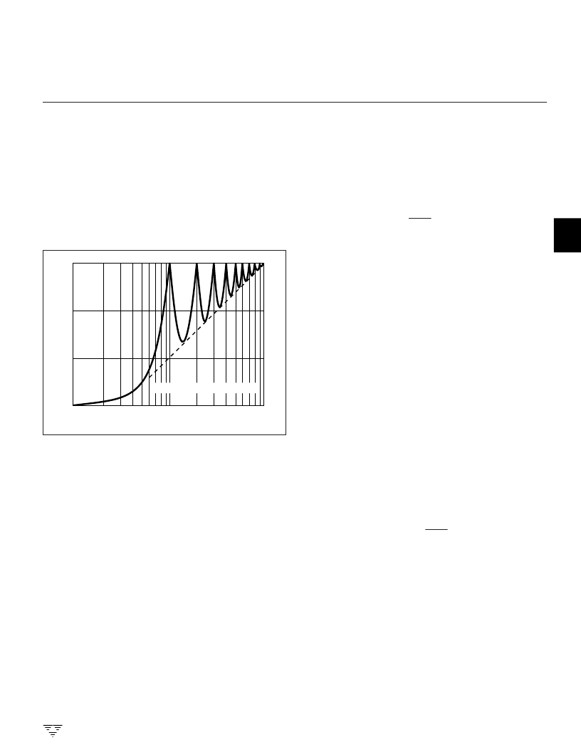
Interfering signals with frequency components at multiples
of the averaging period will be attenuated. Integrating ADCs
commonly operate with the signal integration period set to a
multiple of the 50/60 Hz power line period. (Figure 2B)
Figure 2B. Normal-Mode Rejection of Dual Slope Converter
ANALOG SECTION
In addition to the basic signal integrate and deintegrate
cycles discussed, the circuit incorporates an auto-zero
cycle. This cycle removes buffer amplifier, integrator, and
comparator offset voltage error terms from the conversion.
A true digital zero reading results without adjusting external
potentiometers. A complete conversion consists of three
cycles: an auto-zero, signal-integrate and reference-inte-
grate cycle.
Auto-Zero Cycle
During the auto-zero cycle the differential input signal is
disconnected from the circuit by opening internal analog
gates. The internal nodes are shorted to analog common
(ground) to establish a zero-input condition. Additional ana-
log gates close a feedback loop around the integrator and
comparator. This loop permits comparator offset voltage
error compensation. The voltage level established on C
AZ
compensates for device offset voltages. The offset error
referred to the input is less than 10
μ
V.
The auto-zero cycle length is 1000 to 3000 counts.
30
20
10
0
N
0.1/T
1/T
10/T
INPUT FREQUENCY
T = MEASUREMENT PERIOD
Signal Integrate Cycle
When the auto-zero loop is opened, the internal differ-
ential inputs connect to V
+
signal is integrated for a fixed time period. The signal
integration period is 1000 counts. The externally set clock
frequency is divided by four before clocking the internal
counters. The integration time period is:
IN
and V
–
. The differential input
T
SI
=
x 1000
where:
f
OSC
= External Clock Frequency
The differential input voltage must be within the device
common-mode range (1V of either supply) when the con-
verter and measured system share the same power supply
common (ground). If the converter and measured system do
not share the same power supply common, V
–
tied to analog common.
Polarity is determined at the end of the signal integrate
phase. The sign bit is a true polarity indication in that signals
less than 1 LSB are correctly determined. This allows
precision null detection, limited only by device noise and
auto-zero residual offsets.
IN
should be
Reference Integrate Cycle
The final phase is reference integrate or de-integrate.
–
is internally connected to analog common and V
+
connected across the previously charged reference capaci-
tor. Circuitry within the chip ensures that the capacitor will be
connected with the correct polarity to cause the integrator
output to return to zero. The time required for the output to
return to zero is proportional to the input signal and is
between 0 and 2000 counts. The digital reading displayed is:
V
IN
is
DIGITAL SECTION (TC7106A)
The TC7106A (Figure 3) contains all the segment driv-
ers necessary to directly drive a 3 -1/2 digit liquid crystal
display (LCD). An LCD backplane driver is included. The
backplane frequency is the external clock frequency divided
by 800. For three conversions/second the backplane fre-
quency is 60Hz with a 5V nominal amplitude. When a
segment driver is in phase with the backplane signal the
segment is “OFF.” An out of phase segment drive signal
causes the segment to be “ON” or visible. This AC drive
configuration results in negligible DC voltage across each
LCD segment. This insures long LCD display life. The
polarity segment driver is “ON” for negative analog inputs. If
V
+
IN
and V
–
IN
are reversed, this indicator will reverse.
4
f
OSC
1000 x
V
IN
V
REF
TC7106
TC7106A
TC7107
TC7107A
3-1/2 DIGIT A/D CONVERTERS
相關(guān)PDF資料 |
PDF描述 |
|---|---|
| TC7107ACLW | 3-1/2 DIGIT A/D CONVERTERS |
| TC7107ACPL | 3-1/2 DIGIT A/D CONVERTERS |
| TC7106AIJL | Circular Connector; No. of Contacts:66; Series:MS27473; Body Material:Aluminum; Connecting Termination:Crimp; Connector Shell Size:18; Circular Contact Gender:Socket; Circular Shell Style:Straight Plug; Insert Arrangement:18-66 RoHS Compliant: No |
| TC7107AIJL | JT 66C 66#22M SKT PLUG |
| TC7107IJL | PTB 26C 26#20 PIN/SKT REC |
相關(guān)代理商/技術(shù)參數(shù) |
參數(shù)描述 |
|---|---|
| TC7107CPL | 制造商:Microchip Technology Inc 功能描述:Leaded Process Compatible:No |
| TC7107CPL | 制造商:Microchip Technology Inc 功能描述:3.5 DIGIT ADC CMOS 7107 DIP40 制造商:Microchip Technology Inc 功能描述:3.5 DIGIT ADC, CMOS, 7107, DIP40 制造商:Microchip Technology Inc 功能描述:3.5 DIGIT ADC, CMOS, 7107, DIP40; Resolution (Bits):3.5bit; Supply Voltage Type:Single; Supply Voltage Max:5V; Supply Current:800A; Digital IC Case Style:DIP; No. of Pins:40; Input Channel Type:Differential; Data Interface:Parallel;;RoHS Compliant: Yes |
| TC7107IJL | 功能描述:LED顯示驅(qū)動(dòng)器 3-1/2 Digit A/D w/ LED Driver RoHS:否 制造商:Micrel 數(shù)位數(shù)量:5 片段數(shù)量: 安裝風(fēng)格:SMD/SMT 封裝 / 箱體:PLCC-44 工作電源電壓:4.75 V to 11 V 最大電源電流:10 mA 最大工作溫度:+ 85 C 最小工作溫度:- 40 C 封裝:Tube |
| TC7107IPL | 功能描述:LED顯示驅(qū)動(dòng)器 w/LED Driver RoHS:否 制造商:Micrel 數(shù)位數(shù)量:5 片段數(shù)量: 安裝風(fēng)格:SMD/SMT 封裝 / 箱體:PLCC-44 工作電源電壓:4.75 V to 11 V 最大電源電流:10 mA 最大工作溫度:+ 85 C 最小工作溫度:- 40 C 封裝:Tube |
| TC7107RCPL | 功能描述:LED顯示驅(qū)動(dòng)器 w/LED Driver RoHS:否 制造商:Micrel 數(shù)位數(shù)量:5 片段數(shù)量: 安裝風(fēng)格:SMD/SMT 封裝 / 箱體:PLCC-44 工作電源電壓:4.75 V to 11 V 最大電源電流:10 mA 最大工作溫度:+ 85 C 最小工作溫度:- 40 C 封裝:Tube |
發(fā)布緊急采購(gòu),3分鐘左右您將得到回復(fù)。