- 您現(xiàn)在的位置:買賣IC網 > PDF目錄225281 > TC7662AIJA SWITCHED CAPACITOR CONVERTER, 12 kHz SWITCHING FREQ-MAX, CDIP8 PDF資料下載
參數資料
| 型號: | TC7662AIJA |
| 元件分類: | 穩(wěn)壓器 |
| 英文描述: | SWITCHED CAPACITOR CONVERTER, 12 kHz SWITCHING FREQ-MAX, CDIP8 |
| 封裝: | CERDIP-8 |
| 文件頁數: | 3/7頁 |
| 文件大小: | 53K |
| 代理商: | TC7662AIJA |

3
CHARGE PUMP DC-TO-DC CONVERTER
TC7662A
TC7662A-5 9/11/96
2001 Microchip Technology Inc.
DS21468
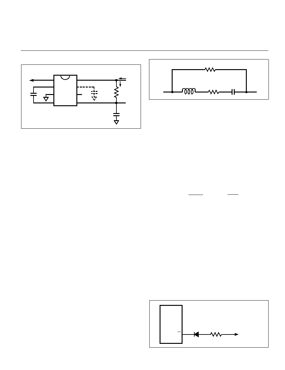
Note one of its characteristics is ESR (equivalent series
resistance). This parasitic resistance winds up in series with
the load. Thus, both voltage and power conversion effi-
ciency are compromised if a low ESR capacitor is not used.
For example, in the "Test Circuit", changing CP and CR
capacitors from typical ESR to low ESR types, the effective
converter output impedance changed from 45
to 40, an
improvement of 12%.
This applies to all types of capacitors, including film
types (polyester, polycarbonate etc.).
Some applications information suggests that the ca-
pacitor is not critical and attributes the limiting factor to the
capacitor's reactance value. Let's examine this:
where DS (duty cycle) = 50%.
Thus, ZC ≈ 1.33 at f = 12kHz, where C = 10F.
For the TC7662A, f = 12,000Hz, and a typical value of
C would be 10
F. This is a reactive impedance of ≈1.33.
If the ESR is as great as 5
, the reactive value is not as
critical as it would first appear, since the ESR would dominate.
The 5
value is typical of a general-purpose electrolytic
capacitor.
Synchronizing
The TC7662A may be synchronized by connecting pin
7 of the TC7662A through a 100k resistor in series with a
diode to a negative-going pulse source. The negative pulse
voltage can be +5V with a 5 microsecond duration going
negative to 0V.
TEST CIRCUIT
Figure 2.
Synchronization
XC =
and ZC =
,
XC
DS
APPLICATIONS INFORMATION
Theory of Operation
The TC7662A is a capacitive charge pump (some-
times called a switched-capacitor circuit), where four
MOSFET switches control the charge and discharge of a
capacitor.
The functional diagram (page 1) shows how the switch-
ing action works. SW1 and SW2 are turned on simulta-
neously, charging C1 to the supply voltage, VDD. This
assumes that the ON resistance of the MOSFETs in series
with the capacitor produce a charging time (3 time con-
stants) less than the ON time provided by the oscillator
frequency, as shown:
3 (RDS(ON) C1) <C1/(0.5 fOSC).
In the next cycle, SW1 and SW2 are turned OFF and,
after a very short interval with all switches OFF (preventing
large currents from occurring due to cross conduction),
SW3 and SW4 are turned ON. The charge in C1 is then
transferred to COUT, BUT WITH THE POLARITY IN-
VERTED. In this way, a negative voltage is derived.
An oscillator supplies pulses to a flip-flop that is fed to a
set of level shifters. These level shifters then drive each set
of switches at one-half the oscillator frequency.
The oscillator has a pin that controls the frequency of
oscillation. Pin 7 can have a capacitor added that is con-
nected to ground. This will lower the frequency of the
oscillator by adding capacitance to the internal timing ca-
pacitor of the TC7662A. (See Oscillator Frequency vs. CEXT,
page 5.)
Capacitors
In early charge pump converters, capacitors were not
considered critical due to the high RDS(ON) of the MOSFET
switches. In order to understand this, let’s look at a model of
a typical electrolytic capacitor (Figure 1).
1
2
πf C
TC7662A
1
2
3
4
8
7
5
CP
+
10
F
COSC
R L
V
(–5V)
OUT
10
F
C R
I L
IS
V
(+5V)
+
NC
6
+
TTL
Q
100 k
TO PIN 7
TC7662A
Figure 1.
Capacitor Equivalent Circuit
EPR
ESL
ESR
C
相關PDF資料 |
PDF描述 |
|---|---|
| TCET1108G | 1 CHANNEL TRANSISTOR OUTPUT OPTOCOUPLER |
| TCFGA0G106K8R | Chip tantalum capacitors with open-function built-in |
| TCFGA0G106M8R | Chip tantalum capacitors with open-function built-in |
| TCFGA0J106K8R | Chip tantalum capacitors with open-function built-in |
| TCFGA0J106M8R | Chip tantalum capacitors with open-function built-in |
相關代理商/技術參數 |
參數描述 |
|---|---|
| TC7662AMJA | 功能描述:電荷泵 High Voltage RoHS:否 制造商:Maxim Integrated 功能:Inverting, Step Up 輸出電壓:- 1.5 V to - 5.5 V, 3 V to 11 V 輸出電流:100 mA 電源電流:1 mA 最大工作溫度:+ 70 C 封裝 / 箱體:SOIC-8 Narrow 封裝:Tube |
| TC7662B | 制造商:MICROCHIP 制造商全稱:Microchip Technology 功能描述:CHARGE PUMP DC-TO-DC VOLTAGE CONVERTER |
| TC7662BC0A | 制造商:Texas Instruments 功能描述: |
| TC7662BCOA | 功能描述:電荷泵 High Voltage RoHS:否 制造商:Maxim Integrated 功能:Inverting, Step Up 輸出電壓:- 1.5 V to - 5.5 V, 3 V to 11 V 輸出電流:100 mA 電源電流:1 mA 最大工作溫度:+ 70 C 封裝 / 箱體:SOIC-8 Narrow 封裝:Tube |
| TC7662BCOA | 制造商:Microchip Technology Inc 功能描述:DC/DC CONVERTER SMD 7662 SOIC8 |
發(fā)布緊急采購,3分鐘左右您將得到回復。