- 您現(xiàn)在的位置:買賣IC網(wǎng) > PDF目錄371180 > TDA10085 (NXP Semiconductors N.V.) Single chip DVB-S/DSS channel receiver PDF資料下載
參數(shù)資料
| 型號: | TDA10085 |
| 廠商: | NXP Semiconductors N.V. |
| 元件分類: | 接收器 |
| 英文描述: | Single chip DVB-S/DSS channel receiver |
| 中文描述: | 單芯片DVB-S/DSS頻道接收機(jī) |
| 文件頁數(shù): | 7/16頁 |
| 文件大小: | 93K |
| 代理商: | TDA10085 |
2001 Aug 31
7
Philips Semiconductors
Product specification
Single chip DVB-S/DSS channel receiver
TDA10085HT
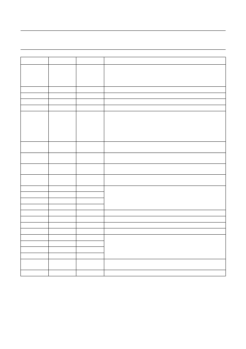
Notes
1.
2.
TTL, 5 V tolerant input (if VDDE5 is connected to 5 V).
DGND, VSSI and VSSE can be connected to the same ground plane.
TDO
41
I/O
boundary scan mode: test data serial output; output provided on the
falling edge of TCK
serial mode enabled (ENSERI = 1): serial TS enable input; must be
set to VSS when not in serial mode
analog supply voltage for the 2nd PLL (typically 1.8 V)
analog ground voltage for the 2nd PLL
digital supply voltage (typically 3.3 V)
digital ground voltage; see note 2
asynchronous, active LOW input that clears the TDA10085; when
CLB# goes LOW the circuit immediately enters its RESET mode and
normal operation resumes three XIN rising edges later after CLB#
returns HIGH; at RESET, the I
2
C-bus register contents are all
initialized to their default values; the minimum width of CLB# LOW
level is three XIN clock periods; pin CLB# is not TTL, 5 V tolerant
packet sync output signal goes HIGH on a rising edge of OCLK each
time the first byte of a packet is provided
uncorrectable packet output signal goes HIGH on a rising edge of
OCLK when the packet provided is uncorrectable
data enable; this output signal is HIGH when there is valid data on
bus DO[7:0]
output clock for the parallel DO[7:0] outputs; OCLK is generated
internally and depends on which interface type is selected
transport stream data output bits; part of the 8-bit parallel data output
after demodulation, Viterbi decoding, de-interleaving, RS decoding
and de-scrambling; possible output interfaces are three parallel and
two serial
ADVD
ADVS
VDDE
VSSE
CLB#
42
43
44
45
46
supply
ground
supply
ground
I
PSYNC
47
O
UNCOR
48
O
DEN
49
O
OCLK
50
O
DO0
DO1
DO2
DO3
VDDI
VSSI
VDDE
VSSE
DO4
DO5
DO6
DO7
22K
51
52
53
54
55
56
57
58
59
60
61
62
63
O
O
O
O
supply
ground
supply
ground
O
O
O
O
O
digital core supply voltage (typically 1.8 V)
digital core ground voltage; see note 2
digital supply voltage (typically 3.3 V)
digital ground voltage; see note 2
transport stream data output bits; part of the 8-bit parallel data output
after demodulation, Viterbi decoding, de-interleaving, RS decoding
and de-scrambling; possible output interfaces are three parallel and
two serial
22 kHz output used to control the antenna LNB (output is controlled
via the I
2
C-bus interface)
digital core ground voltage; see note 2
VSSI
64
ground
SYMBOL
PIN
TYPE
DESCRIPTION
相關(guān)PDF資料 |
PDF描述 |
|---|---|
| TDA10085HT | Single chip DVB-S/DSS channel receiver |
| TDA1010 | 6 W audio power amplifier in car applications 10 W audio power amplifier in mains-fed applications |
| TDA1010A | 6 W audio power amplifier in car applications 10 W audio power amplifier in mains-fed applications |
| TDA1011 | 2 to 6 W audio power amplifier |
| TDA1013B | 4 W audio power amplifier with DC volume control |
相關(guān)代理商/技術(shù)參數(shù) |
參數(shù)描述 |
|---|---|
| TDA10085HT | 制造商:PHILIPS 制造商全稱:NXP Semiconductors 功能描述:Single chip DVB-S/DSS channel receiver |
| TDA1010 | 制造商:PHILIPS 制造商全稱:NXP Semiconductors 功能描述:6 W audio power amplifier in car applications 10 W audio power amplifier in mains-fed applications |
| TDA1010A | 制造商:PHILIPS 制造商全稱:NXP Semiconductors 功能描述:6 W audio power amplifier in car applications 10 W audio power amplifier in mains-fed applications |
| TDA1011 | 制造商:PHILIPS 制造商全稱:NXP Semiconductors 功能描述:2 to 6 W audio power amplifier |
| TDA1011A | 制造商:PHILIPS 制造商全稱:NXP Semiconductors 功能描述:2 to 5W audio power amplifier with preamplifier |
發(fā)布緊急采購,3分鐘左右您將得到回復(fù)。