- 您現(xiàn)在的位置:買賣IC網(wǎng) > PDF目錄368628 > TDA3504 (NXP SEMICONDUCTORS) Video control combination circuit(視頻匯編電路) PDF資料下載
參數(shù)資料
| 型號(hào): | TDA3504 |
| 廠商: | NXP SEMICONDUCTORS |
| 元件分類: | 消費(fèi)家電 |
| 英文描述: | Video control combination circuit(視頻匯編電路) |
| 中文描述: | SPECIALTY CONSUMER CIRCUIT, PDIP20 |
| 封裝: | 0.300 INCH, PLASTIC, SOT-146-1, DIP-20 |
| 文件頁(yè)數(shù): | 7/12頁(yè) |
| 文件大小: | 108K |
| 代理商: | TDA3504 |
1996 Jan 09
7
Philips Semiconductors
Product specification
Video control combination circuit
TDA3504
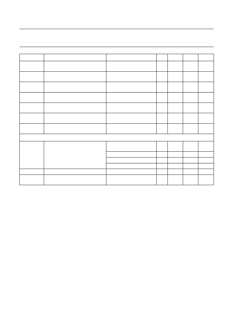
Notes
1.
2.
3.
4.
Maximum value 110 mA after warm-up.
Values are proportional to the supply voltage.
Matrixed according to equation V
(G
Y)
=
0.51V
(R
Y)
0.19V
(B
Y)
.
Clipping due to internal signal limitation may occur when the Y input is greater than nominal and maximum contrast
and minimum brightness.
When V
7-18
< 0.4 V during clamping time, the black levels of the inserted RGB signals are clamped on the black
levels of the internal RGB signals.
When V
7-18
> 0.9 V during clamping time, the black levels of the inserted RGB signals are clamped on an internal
DC voltage (correct clamping of the external RGB signals is possible only when they are synchronous with the
sandcastle pulse).
Internal signal limitation is allowed to start at 5.5 V after warm-up time.
The sandcastle pulse is compared with three internal thresholds (proportional to V
P
) and the given levels separate
the various pulses.
Blanked to ultra-black (
25%).
Pulse duration
≥
3.5
μ
s.
5.
6.
7.
8.
9.
G
v1-15
;
G
v19-14
α
1-15
;
α
19-14
voltage gain with respect to colour
difference inputs (pins 14 and 15)
frequency response of colour
difference paths
voltage gain with respect to inserted
signals
frequency response of inserted
signal paths
difference in transition times
between R, G and B channels
delay time between signal switching
and signal insertion
difference in gain between normal
and signal insertion mode
11
14
17
dB
f = 0 to 2 MHz
3
dB
G
v19-10
;
G
v20-9
; G
v1-8
α
19-10
;
α
20-9
;
α
1-8
t
19, 20, 1
12
14
16
dB
f = 0 to 10 MHz
3
dB
0
15
ns
t
d
25
+25
ns
G
19, 20, 1
10
%
Sandcastle pulse detector (pin 6)
V
6
the following amplitudes are
required for separating the various
pulses
horizontal and vertical
blanking; notes 7 and 8
horizontal; note 7
clamping; notes 7 and 9
no keying; note 7
LOW
2.1
2.5
2.9
V
4.1
7.6
4.5
8.0
0.5
5.0
12.0
1.0
110
V
V
V
μ
A
μ
s
I
I
t
d
input current
delay of leading edge of clamping
pulse
SYMBOL
PARAMETER
CONDITIONS
MIN.
TYP.
MAX.
UNIT
相關(guān)PDF資料 |
PDF描述 |
|---|---|
| TDA3505 | Video control combination circuit with automatic cut-off control(帶自動(dòng)截止電路的視頻控制匯編電路) |
| TDA3506 | Video control combination circuit with automatic cut-off control(帶自動(dòng)截止電路的視頻控制匯編電路) |
| TDA3602 | Multiple output voltage regulator(多路輸出電壓穩(wěn)壓器) |
| TDA3603 | Multiple voltage regulator with switch(帶開(kāi)關(guān)轉(zhuǎn)換的多路輸出穩(wěn)壓器) |
| TDA3604Q | Multiple voltage regulators with external reset delay and switch(外部帶有復(fù)位延遲和開(kāi)關(guān)轉(zhuǎn)換的多路輸出電壓穩(wěn)壓器) |
相關(guān)代理商/技術(shù)參數(shù) |
參數(shù)描述 |
|---|---|
| TDA3505 | 制造商:PHILIPS 制造商全稱:NXP Semiconductors 功能描述:Video control combination circuit with automatic cut-off control |
| TDA3505G | 制造商:未知廠家 制造商全稱:未知廠家 功能描述:Analog IC |
| TDA3506 | 制造商:PHILIPS 制造商全稱:NXP Semiconductors 功能描述:Video control combination circuit with automatic cut-off control |
| TDA3507 | 制造商:PHILIPS 制造商全稱:NXP Semiconductors 功能描述:Video control combination circuit with automatic cut-off control |
| TDA3508 | 制造商:PHILIPS 制造商全稱:NXP Semiconductors 功能描述:Video control combination circuit with automatic cut-off control |
發(fā)布緊急采購(gòu),3分鐘左右您將得到回復(fù)。