- 您現(xiàn)在的位置:買賣IC網(wǎng) > PDF目錄371181 > TDA3609 (NXP Semiconductors N.V.) Multiple voltage regulator with switch and ignition buffers PDF資料下載
參數(shù)資料
| 型號: | TDA3609 |
| 廠商: | NXP Semiconductors N.V. |
| 英文描述: | Multiple voltage regulator with switch and ignition buffers |
| 中文描述: | 多與點火開關(guān)穩(wěn)壓器和緩沖器 |
| 文件頁數(shù): | 5/20頁 |
| 文件大?。?/td> | 136K |
| 代理商: | TDA3609 |

1997 Aug 15
5
Philips Semiconductors
Preliminary specification
Multiple voltage regulator with switch and
ignition buffers
TDA3609JR
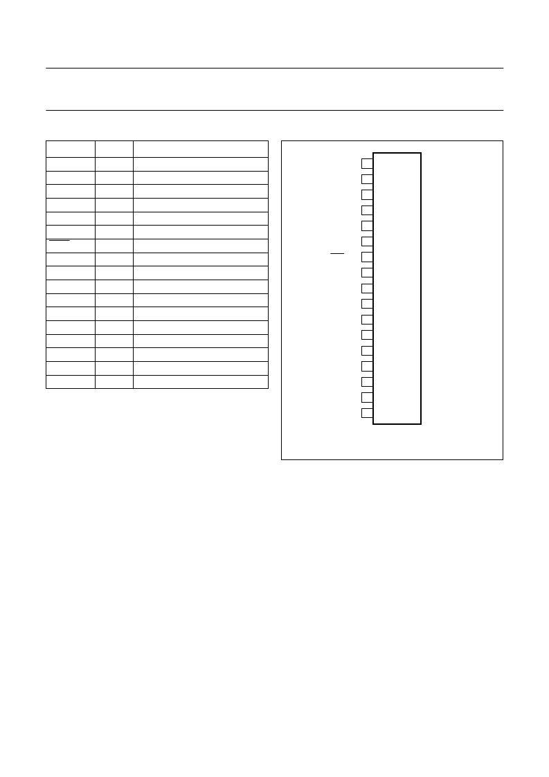
PINNING
SYMBOL
PIN
DESCRIPTION
V
P
REG1
REG3
EN3
IGN2
IN
IGN1
IN
IGN1
OUT
IGN2
OUT
RES
EN1
ENSW
HOLD
C
RES
GND
REG2
BU
SW
1
2
3
4
5
6
7
8
9
supply voltage
regulator 1 output
regulator 3 output
enable input regulator 3
ignition 2 input
ignition 1 input
ignition 1 output (active LOW)
ignition 2 output
reset output
enable input regulator 1
enable input power switch
hold output
reset delay capacitor
ground
regulator 2 output
back-up
power switch output
10
11
12
13
14
15
16
17
Fig.2 Pin configuration.
handbook, halfpage
TDA3609JR
MGK606
VP
REG1
REG3
EN3
IGN2IN
IGN1IN
IGN1OUT
IGN2OUT
RES
EN1
ENSW
HOLD
CRES
GND
REG2
BU
SW
1
2
3
4
5
6
7
8
9
10
11
12
13
14
15
16
17
FUNCTIONAL DESCRIPTION
The TDA3609JR is a multiple output voltage regulator with
a power switch, intended for use in car radios with or
without a microcontroller. Because of low-voltage
operation of the car radio, low-voltage drop regulators are
used in the TDA3609JR.
Regulator 2 will switch on when the back-up voltage
exceeds 6.5 V for the first time and will switch off again
when the output voltage of regulator 2 is below 1.9 V (this
is far below an engine start). When regulator 2 is switched
on and the output voltage of this regulator is within its
voltage range, the reset output will be enabled (reset will
go HIGH via a pull-up resistor) to generate a reset to the
microcontroller. The reset cycles can be extended by a
external capacitor at pin 13. The above mentioned start-up
feature is built-in to secure a smooth start-up of the
microcontroller at first connection, without uncontrolled
switching of regulator 2 during the start-up sequence.
The charge of the back-up capacitor can be used to supply
regulator 2 for a short period when the supply falls down
to 0 V (time depends on value of storage capacitor).
The output stages (regulator 1 and 3) of this regulator have
extreme low noise behaviour and good stability. Using
small output capacitors regulator 1 and 3 are made stable.
When both regulator 2 and the supply voltage (V
P
> 4.5 V)
are available, regulators 1 and 3 can be operated by
means of enable inputs (pins 10 and 4 respectively).
Regulator 1 has a hold output (open collector) indicating
that the output voltage of this regulator is settled (held
HIGH by external pull-up resistor). When the output
voltage of this regulator drops out of regulation (because
of supply voltage drop or high load) the hold output will go
LOW. The hold output signal is only valid when regulator 1
is enabled by its enable input (pin 10).
相關(guān)PDF資料 |
PDF描述 |
|---|---|
| TDA3609JR | Multiple voltage regulator with switch and ignition buffers |
| TDA3651 | VERTICAL DEFLECTION CIRCUIT |
| TDA3651A | VERTICAL DEFLECTION CIRCUIT |
| TDA3651Q | VERTICAL DEFLECTION CIRCUIT |
| TDA3661AT | Very low dropout voltage/quiescent current adjustable voltage regulator |
相關(guān)代理商/技術(shù)參數(shù) |
參數(shù)描述 |
|---|---|
| TDA3609JR | 制造商:PHILIPS 制造商全稱:NXP Semiconductors 功能描述:Multiple voltage regulator with switch and ignition buffers |
| TDA3615J | 制造商:PHILIPS 制造商全稱:NXP Semiconductors 功能描述:Multiple voltage regulator |
| TDA3615J/N2,112 | 功能描述:線性穩(wěn)壓器 - 標(biāo)準(zhǔn) CARRADIO POWER AMPLIFIERS RoHS:否 制造商:STMicroelectronics 輸出類型: 極性: 輸出電壓:1.8 V 輸出電流:150 mA 負(fù)載調(diào)節(jié): 最大輸入電壓:5.5 V 線路調(diào)整率: 最大工作溫度:+ 125 C 安裝風(fēng)格:SMD/SMT 封裝 / 箱體:SOT-323-5L |
| TDA3615J/N2C,112 | 制造商:NXP Semiconductors 功能描述: |
| TDA3616 | 制造商:PHILIPS 制造商全稱:NXP Semiconductors 功能描述:Multiple voltage regulator with battery detection |
發(fā)布緊急采購,3分鐘左右您將得到回復(fù)。