- 您現(xiàn)在的位置:買賣IC網(wǎng) > PDF目錄373622 > TDA7383 (意法半導(dǎo)體) 4 x 30W QUAD BRIDGE CAR RADIO AMPLIFIER PDF資料下載
參數(shù)資料
| 型號(hào): | TDA7383 |
| 廠商: | 意法半導(dǎo)體 |
| 元件分類: | 音頻放大器 |
| 英文描述: | 4 x 30W QUAD BRIDGE CAR RADIO AMPLIFIER |
| 中文描述: | 4個(gè)功率30W的四橋汽車無線電放大器 |
| 文件頁(yè)數(shù): | 8/12頁(yè) |
| 文件大?。?/td> | 339K |
| 代理商: | TDA7383 |
INPUT STAGE
The TDA7383’sinputs are ground-compatibleand
can stand very high inputsignals (
±
8Vpk)without
any performancesdegradation.
If the standard value for the input capacitors
(0.1
μ
F) is adopted, the low frequency cut-off will
amount to 16 Hz.
STAND-BY AND MUTING
STAND-BY and MUTING facilities are both
CMOS-COMPATIBLE. If unused, a straight con-
nection to Vs of theirrespectivepins would be ad-
missible. Conventionallow-power transistors can
be employed to drive muting and stand-by pins in
absence of true CMOSports or microprocessors.
R-C cells have always to be used in order to
smooth down the transitions for preventing any
audible transient noises.
Since a DC current of about 10 uA normally flows
out of pin 22, the maximum allowable muting-se-
ries resistance (R
2
) is 70K
, which is sufficiently
high to permit a muting capacitor reasonably
small (about1
μ
F).
If R
2
is higher than recommended, the involved
risk will be that the voltage at pin 22 may rise to
above the 1.5 V threshold voltage and the device
will consequentlyfail to turn OFF when the mute
line is broughtdown.
About the stand-by, the time constant to be as-
signed in order to obtain a virtually pop-free tran-
sition has to be slower than2.5V/ms.
DIAGNOSTICSFACILITY
The TDA7383 is equipped with a diagnostics cir-
cuitry able to detectthe following events:
CLIPPINGin the output stage
OVERHEATING
proximity)
OUTPUT MISCONNECTIONS (OUT-GND &
OUT-Vs shorts)
Diagnostics information is available across an
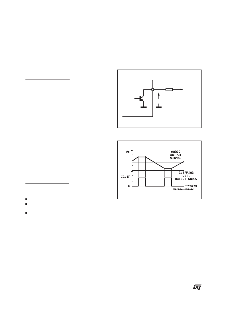
open collector output located at pin 25 (fig. 12)
through a current sinking whenever at least one
of the aboveevents is recognized.
Among them, the
CLIPPING DETECTOR
acts in
a way to output a signal as soon as one or more
power transistorsstart being saturated.
As a result, the clipping-related signal at pin 25
takes the form of pulses, which are perfectly syn-
cronized with each single clipping event in the
music program and reflect the same duration time
(fig. 13).
Applications making use of this facility
usually operatea filtering/integrationof the pulses
train through passive R-C networks and realize a
volume (or tone bass) stepping down in associa-
(THERMAL
SHUT-DOWN
tion with microprocessor-driven audioprocessors.
The maximum load that pin 25 can sustain is
1K
.
Due to its operating principles, the clipping detec-
tor has to be viewed mainly as a power-depend-
Figure12:
Diagnosticscircuit.
ent feature rather than frequency-dependent.This
means that clipping state will be immediately sig-
naled out whenever a fixed power level is
reached,regardlessof the audiofrequency.
In other words, this feature offers the means to
counteract the extremely sound-damaging effects
of clipping, caused by a sudden increase of odd
order harmonics and appearanceof serious inter-
modulationphenomena.
Another possible kind of distortion control could
be the setting of a maximum allowable THD limit
(e.g. 0.5 %) over the entire audio frequency
range. Besides offering no practical advantages,
this procedure cannot be much accurate, as the
non-clipping distortion is likely to vary over fre-
quency.
In case of
OVERHEATING
, pin 25 will signal out
the junction temperature proximity to the thermal
shut-down threshold. This will typically start about
2
o
C before the thermal shut-down threshold is
VREF
R
Vpin 25
25
D95AU303A
Figure13:
ClippingDetection Waveforms.
TDA7383
8/12
相關(guān)PDF資料 |
PDF描述 |
|---|---|
| TDA7384 | 4 x 35W QUAD BRIDGE CAR RADIO AMPLIFIER |
| TDA7384A | 4 x 35W QUAD BRIDGE CAR RADIO AMPLIFIER |
| TDA7385 | 4 x 30W QUAD BRIDGE CAR RADIO AMPLIFIER |
| TDA7386 | 4 x 40W QUAD BRIDGE CAR RADIO AMPLIFIER |
| TDA7391 | 35W BRIDGE CAR RADIO AMPLIFIER |
相關(guān)代理商/技術(shù)參數(shù) |
參數(shù)描述 |
|---|---|
| TDA7384 | 制造商:STMICROELECTRONICS 制造商全稱:STMicroelectronics 功能描述:4 x 35W QUAD BRIDGE CAR RADIO AMPLIFIER |
| TDA7384A | 功能描述:音頻放大器 4X35W Quad Brdg Amp RoHS:否 制造商:STMicroelectronics 產(chǎn)品:General Purpose Audio Amplifiers 輸出類型:Digital 輸出功率: THD + 噪聲: 工作電源電壓:3.3 V 電源電流: 最大功率耗散: 最大工作溫度: 安裝風(fēng)格:SMD/SMT 封裝 / 箱體:TQFP-64 封裝:Reel |
| TDA7384A_07 | 制造商:STMICROELECTRONICS 制造商全稱:STMicroelectronics 功能描述:4 x 42W quad bridge car radio amplifier |
| TDA7384B | 功能描述:音頻放大器 Car-Radio Amplifier 18V Op 28V DC 36W RoHS:否 制造商:STMicroelectronics 產(chǎn)品:General Purpose Audio Amplifiers 輸出類型:Digital 輸出功率: THD + 噪聲: 工作電源電壓:3.3 V 電源電流: 最大功率耗散: 最大工作溫度: 安裝風(fēng)格:SMD/SMT 封裝 / 箱體:TQFP-64 封裝:Reel |
| TDA7385 | 功能描述:音頻放大器 4X30W Quad Brdg Amp RoHS:否 制造商:STMicroelectronics 產(chǎn)品:General Purpose Audio Amplifiers 輸出類型:Digital 輸出功率: THD + 噪聲: 工作電源電壓:3.3 V 電源電流: 最大功率耗散: 最大工作溫度: 安裝風(fēng)格:SMD/SMT 封裝 / 箱體:TQFP-64 封裝:Reel |
發(fā)布緊急采購(gòu),3分鐘左右您將得到回復(fù)。