- 您現(xiàn)在的位置:買賣IC網 > PDF目錄371182 > TDA8020 (NXP Semiconductors N.V.) Dual smart card interface PDF資料下載
參數資料
| 型號: | TDA8020 |
| 廠商: | NXP Semiconductors N.V. |
| 英文描述: | Dual smart card interface |
| 中文描述: | 雙界面智能卡 |
| 文件頁數: | 9/24頁 |
| 文件大?。?/td> | 114K |
| 代理商: | TDA8020 |

2001 Aug 15
9
Philips Semiconductors
Product specification
Dual smart card interface
TDA8020HL
R
EADING STATUS
START, ADDRESS, READ, STATUS byte, STOP.
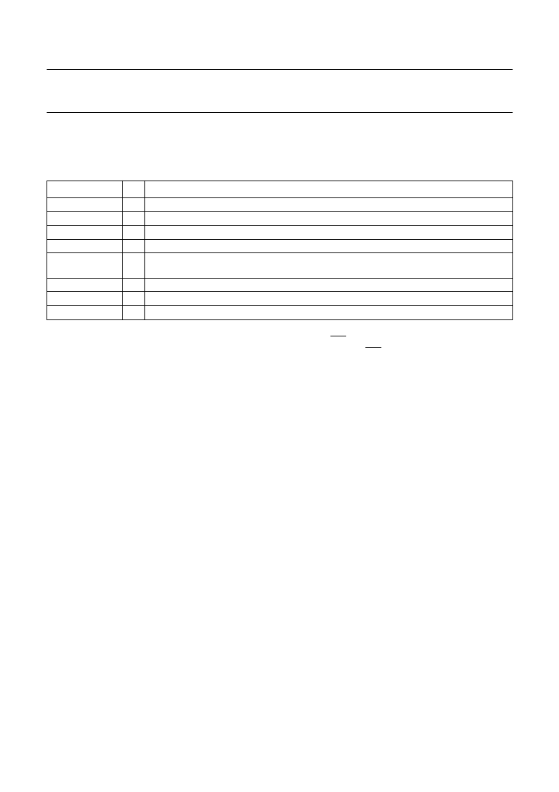
Table 4
STATUS bits (all bits cleared after power-on, except SUPL and PRES)
When one of the bits PRESL, MUTE, EARLY and PROT is set, then pin IRQ goes LOW until the status byte has been
read. After power-on, bit SUPL is set until the status byte has been read, and pin IRQ is LOW until the supervisor
becomes inactive.
NAME
BIT
DESCRIPTION
PRES
PRESL
I/O
SUPL
PROT
0
1
2
3
4
set when the card is present; reset when the card is not present
set when the card has been inserted or extracted; reset when the status has been read
set when I/O is HIGH and reset if I/O is LOW
set when the supervisor has signalled a fault; reset when the status has been read
set when an overload or an overheating has occurred during a session; reset when the
status has been read
set during ATR when the selected card has not answered during the ISO 7816 time slots
set during ATR when the selected card has answered too early
set if the card is active; reset if the card is inactive
MUTE
EARLY
ACTIVE
5
6
7
DC/DC converter
V
CC1
is the supply voltage for card 1 contacts, V
CC2
for
card 2 contacts. Card 1 and card 2 may be independently
powered-down, powered at 5 V or powered at 3 V. A
capacitor type step-up converter is used for generating
these voltages. This step-up converter acts either as a
doubler, tripler or follower.
If V
CC
is the maximum value of V
CC1
and V
CC2
, then there
are 4 possible situations:
V
DD
= 3 V and V
CC
= 3 V: in this case, the DC/DC
converter acts as a doubler with a regulation of
approximately 4.0 V
V
DD
= 3 V and V
CC
= 5 V: in this case, the DC/DC
converter acts as a tripler with a regulation of
approximately 5.5 V
V
DD
= 5 V and V
CC
= 3 V: in this case, the DC/DC
converter acts as a follower: V
DD
is applied on V
UP
V
DD
= 5 V and V
CC
= 5 V: in this case, the DC/DC
converter acts as a doubler with a regulation of
approximately 5.5 V.
The switch between the modes is automatically executed
when V
DD
is approximately 3.4 V.
Each card may independently draw a current up to 65 mA,
also during activation, with a supply voltage from 2.5 V up
to 6.5 V provided the sum of I
CC1
and I
CC2
does not
exceed 80 mA.
If V
DD
> 3 V, for 5 V cards, then both cards can draw up to
55 mA at the same time.
If V
DD
> 3.3 V, for 3 V cards, then both cards can draw up
to 50 mA at the same time.
The DC/DC converter is powered with specific pins (V
DDA
and AGND) to enable separate decoupling.
The output voltage, V
UP
, is internally fed to the V
CC
generators. V
CC1
, V
CC2
and CGND1, CGND2 are used as
a reference for all other cards contacts.
Sequencers and clock counter
Two sequencers are used to ensure activation and
deactivation sequences according to ISO 7816 and
EMV norms, even in the event of an emergency (card
removal during transaction, supply drop-out and hardware
problem).
The sequencers are clocked by the internal oscillator.
The activation of a card is initiated by setting the card
select bit and the start bit within the control register. This is
only possible if the card is present and if the voltage
supervisor is not active.
During activation the DC/DC converter is initiated (except
if another card is already powered up or if V
DD
= 5 V and
V
CC
= 3 V). V
CC
then goes high to the selected voltage
(3 or 5 V), the I/O lines are then enabled and the clock is
started with RST LOW.
相關PDF資料 |
PDF描述 |
|---|---|
| TDA8260 | Satellite Zero-IF QPSK/8PSK downconverter with PLL synthesizer |
| TDA8260TW | Satellite Zero-IF QPSK/8PSK downconverter with PLL synthesizer |
| TDA8304 | SMALL SIGNAL COMBINATION IC FOR COLOUR TV |
| TDA8315 | Integrated NTSC decoder and sync processor |
| TDA8315T | Integrated NTSC decoder and sync processor |
相關代理商/技術參數 |
參數描述 |
|---|---|
| TDA8020HL | 制造商:PHILIPS 制造商全稱:NXP Semiconductors 功能描述:Dual smart card interface |
| TDA8020HL/C1,118 | 功能描述:輸入/輸出控制器接口集成電路 SMART CARD INTERFACE RoHS:否 制造商:Silicon Labs 產品: 輸入/輸出端數量: 工作電源電壓: 最大工作溫度:+ 85 C 最小工作溫度:- 40 C 安裝風格:SMD/SMT 封裝 / 箱體:QFN-64 封裝:Tray |
| TDA8020HL/C2 | 制造商:NXP Semiconductors 功能描述:Cut Tape |
| TDA8020HL/C2,118 | 功能描述:輸入/輸出控制器接口集成電路 SMART CARD INTERFACE DUAL RoHS:否 制造商:Silicon Labs 產品: 輸入/輸出端數量: 工作電源電壓: 最大工作溫度:+ 85 C 最小工作溫度:- 40 C 安裝風格:SMD/SMT 封裝 / 箱體:QFN-64 封裝:Tray |
| TDA8020HL/C2,151 | 功能描述:接口 - 專用 Dual IC card interface RoHS:否 制造商:Texas Instruments 產品類型:1080p60 Image Sensor Receiver 工作電源電壓:1.8 V 電源電流:89 mA 最大功率耗散: 最大工作溫度:+ 85 C 安裝風格:SMD/SMT 封裝 / 箱體:BGA-59 |
發(fā)布緊急采購,3分鐘左右您將得到回復。