- 您現(xiàn)在的位置:買賣IC網(wǎng) > PDF目錄373626 > TDA9102C (意法半導體) H/V PROCESSOR FOR TTL V.D.U PDF資料下載
參數(shù)資料
| 型號: | TDA9102C |
| 廠商: | 意法半導體 |
| 英文描述: | H/V PROCESSOR FOR TTL V.D.U |
| 中文描述: | 水平/垂直處理器的TTL顯示單元 |
| 文件頁數(shù): | 3/7頁 |
| 文件大小: | 84K |
| 代理商: | TDA9102C |
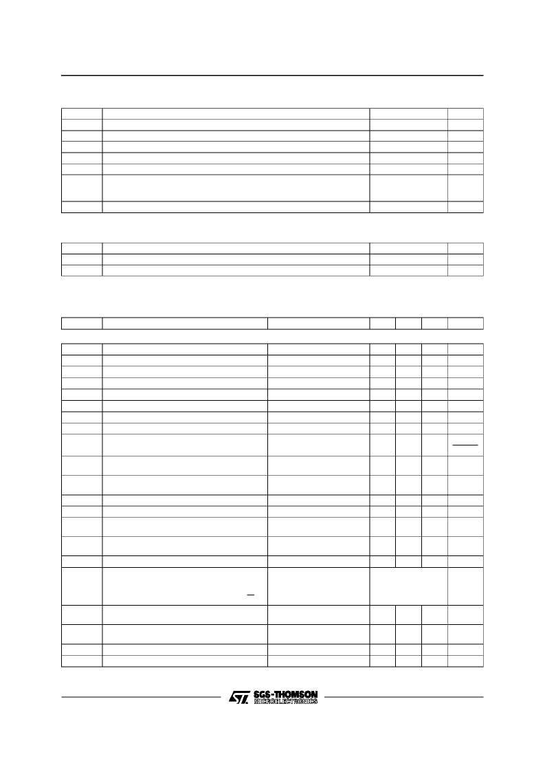
ABSOLUTE MAXIMUM RATINGS
Symbol
V
S
V
SYNC
I
OH
I
15
I
19
P
TOT
Parameter
Value
18
+ V
S
2
- 10
- 10
Unit
V
V
A
mA
mA
Supply Voltage
Sync Input Peak Voltage
Output Sinking Peak Current (Pin 7 ; t < 3
μ
s)
Output Current (Pin15)
Output Current (Pin19)
Total power dissipation
G
T
amb
< 70
o
C
G
T
pin
< 90
o
C
Storage and JunctionTemperature
1.4
1.5
W
W
o
C
T
STG
, T
J
- 40 to 150
9
THERMAL DATA
Symbol
R
TH(J-C)
R
TH(J-A)
Parameter
Value
40
55
Unit
o
C/W
o
C/W
Junction-case Thermal Resistance
Junction-ambient Thermal Resistance
9
ELECTRICALCHARACTERISTICS
(T
AMB
= 25
o
C, V
S
= 12V,refer to thetest circuits, unless otherwisespecified)
Symbol
HORIZONTAL SECTION
V
S
I
S
V
1
I
1
V
2
K
0
V
3
- V
1
I
3
K
3
Parameter
Test conditions
Min.
Typ.
Max.
Unit
Supply Voltage Range
Supply Current
Voltage Reference at Pin 1
Current at Pin 1
Voltage Swing at Pin 2
Control Voltage Range
Peak Control Current
Gain PhaseComparator
φ
1
K
3
= 2 x I
3
/ 360
Sync Threshold Input (neg. edge)
10.5
12
40
3.5
15.5
70
3.8
V
mA
V
mA
V
PP
I
1
= 0.5mA
3.2
- 1
3.7
2.8
1.6
4
4.3
3.2
f
o
= 1/(K
0
x R1 x C2)
(See technical note 1)
3.04
2.5
3
17
V
mA
μ
A
degree
V
V
μ
A
μ
A
μ
s
V
μ
s
V
4
G
Sync high
G
Sync low
G
Input high
G
Input low
@ f
H
= 27.64kHz
2
8
0.8
10
I
4
Current at Pin 4
- 10
1
5.6
T
4
V
5
t
5
Input Pulse Duration T = 1/f
H
Monostable Threshold
Internal Pulse Width (t
5
= C5 x V
5
/I
5
)
0.9T
6.4
6
C5 = 220 pF
(see technical note 2)
f
H
= 27kHz
f
H
= 70kHz
I
7
= 600 mA
See technical note 4
@ f
H
= 27kHz
3.6
t
7
Output PulseDuration (low) - T = 1/f
H
0.38T
0.35T
0.41T
0.39T
1.2
0.44T
0.43T
2.5
μ
s
μ
s
V
s
V
7
sat
t
D
Output Saturation Voltage
Permissible delay betweenoutput pulse
leading edge and flyback pulse leading edge
(for keeping a constant duty cycle) ; T
=
1
f
H
0.41 T - t
FLY
I
FLY
Flyback Input Current at Pin 8
G
Flyback On
G
Flyback Off
G
I
8=
1mA
G
I
8
= - 1mA
0.7
-1
0.6
2
mA
mA
V
V
mA
mA
V
8
Clamp voltage at Pin 8
- 0.6
2
I
8
Current for switching low the output pulse
Peak control current
0.7
I
9
0.9
9
TDA9102C
3/7
相關(guān)PDF資料 |
PDF描述 |
|---|---|
| TDA9109A | LOW-COST I2C CONTROLLED DEFLECTION PROCESSOR FOR MULTISYNC MONITOR |
| TDA9109N | LOW-COST DEFLECTION PROCESSOR FOR MULTISYNC MONITORS |
| TDA9109SN | LOW-COST DEFLECTION PROCESSOR FOR MULTISYNC MONITORS |
| TDA9109 | LOW-COST DEFLECTION PROCESSOR FOR MULTISYNC MONITORS |
| TDA9109S | LOW-COST DEFLECTION PROCESSOR FOR MULTISYNC MONITORS |
相關(guān)代理商/技術(shù)參數(shù) |
參數(shù)描述 |
|---|---|
| TDA9102CT | 制造商:STMICROELECTRONICS 制造商全稱:STMicroelectronics 功能描述:H/V PROCESSOR FOR TTL V.D.U |
| TDA9102F | 制造商:STMICROELECTRONICS 制造商全稱:STMicroelectronics 功能描述:H/V PROCESSOR FOR TTL V.D.U |
| TDA9102T | 制造商:STMICROELECTRONICS 制造商全稱:STMicroelectronics 功能描述:H/V PROCESSOR FOR TTL V.D.U |
| TDA9103 | 制造商:SGS 功能描述: |
| TDA9105 | 制造商:Panasonic Industrial Company 功能描述:IC |
發(fā)布緊急采購,3分鐘左右您將得到回復。