- 您現(xiàn)在的位置:買賣IC網(wǎng) > PDF目錄373630 > TEA7092TQ (意法半導(dǎo)體) TELEPHONE ANALOG FRONT END PDF資料下載
參數(shù)資料
| 型號: | TEA7092TQ |
| 廠商: | 意法半導(dǎo)體 |
| 英文描述: | TELEPHONE ANALOG FRONT END |
| 中文描述: | 電話模擬前端 |
| 文件頁數(shù): | 17/57頁 |
| 文件大?。?/td> | 574K |
| 代理商: | TEA7092TQ |
第1頁第2頁第3頁第4頁第5頁第6頁第7頁第8頁第9頁第10頁第11頁第12頁第13頁第14頁第15頁第16頁當(dāng)前第17頁第18頁第19頁第20頁第21頁第22頁第23頁第24頁第25頁第26頁第27頁第28頁第29頁第30頁第31頁第32頁第33頁第34頁第35頁第36頁第37頁第38頁第39頁第40頁第41頁第42頁第43頁第44頁第45頁第46頁第47頁第48頁第49頁第50頁第51頁第52頁第53頁第54頁第55頁第56頁第57頁
I
L
(mA)
0
20
10
40
30
60
50
80
70
100
90
I
L
(
I
LS
Ip
IVMC
0
20
40
60
80
100
120
0
2
4
6
8
10
A
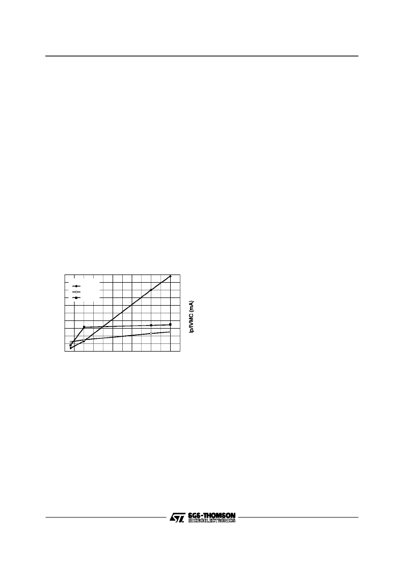
Figure21
II - SPEECHFEATURES
(continued)
II.1.4 - Further Information
(V
CC
/ V
REF
/ I
REF
/ V
MC
/ V
RMC
/ V
LS
/ V
REFL
)
For moreinformation on thesepins see Section I.4 - Input/outputConfigurations.
V
CC
(Pin 26) , V
REF
(Pin25) , I
REF
(Pin 29)
The V
CC
supplies the transmit path, handset and
handfree microphone amplifiers, the receive path,
earphoneamplifier and thetransmit squelch/antia-
coustic feedbackstage.
The current consumptionon this pin, I
P
, is 1.3mA
at a20mA line current (see Figure 21).
From the V
CC
supply, the V
REF
stageis built. V
REF
is usedasan AC ground forall thestagespowered
from V
CC
.
The outputcurrent compliance of V
REF
is :
±
1mA.
The referencevoltage at V
REF
is : V
CC
/2.
I
REF
Pin is used as an internal current reference.
The R2 value is fixedand should not be modified.
It is recommended to connecta
±
1%resistor value
on thispin.
The voltage at I
REF
pin has a 300mV constant
value.
V
MC
(Pin2) , V
RMC
(Pin 8)
These 2 pins supply the microcontroller. These
2 pinsare connectedthrough a serial regulator.
On V
MC
a 470
μ
F capacitor is connected, this ca-
pacitor is chargedonly when TEA7092 ispowered
from Pin V
L
(Pin3) (OFF-HOOKstate) and is used
to power supply the microcontroller during pulse
dialing, flash and earth button, when the line loop
is open.
As described in Section II.1.3, this capacitor is
quicklycharged during the ”Start up” condition.
The DC value at V
MC
is :
V
MC
= V
L
- 0.4V
and is internally limited at 6V max.
V
RMC
is powered from the highest DC value be-
tween Pin V
LS
(Pin 1) and Pin V
MC
(Pin 2) in
OFF-HOOK state or from Pin V
LS
(Pin 1) in ring
mode.
V
RMC
is a 3.5Vstabilized power supply.
V
RMC
suppliesthe oscillator, the logic part (Micro-
controllerinterface, errorbeep, and ring frequency
generators) and the logic part of the D.A.C. used
for the waiting melody and the DTMF generators.
Thecurrentconsumptiononthispinis 250
μ
Awhen
the oscillator is ONand 50
μ
Awhen theoscillator is
OFF code (0111010)is sent.
Note :
To reduce the C10 value connected at
PinV
MC
(Pin 2), it is recommended to inhibit the
oscillatorduringthe pulse dialingandflash signali-
zations.
In ring mode only the 4.7
μ
F capacitor connected
on Pin V
RMC
(Pin8) is charged to achievea short
delay to generate the ring signal on the loud-
speaker.
V
LS
(Pin1) , V
REFL
(Pin 4)
The V
LS
supplies the loudspeaker amplifier part.
The current source,I
LS
, betweenthe Pin V
L
(Pin3)
and the Pin V
LS
(Pin 1) gives the main part of the
line current to supply the loudspeaker amplifier
(seeFigure 21) :
I
LS
= 0.74 x I
L
- 1.8mA; for I
L
< 15mA
I
LS
= 0.92 x I
L
- 4.5mA; for I
L
> 15mA
The internal current consumption on V
LS
is 1mA,
so the current I
LS1
available for the loudspeaker
and other peripheralsis :
I
LS1
= I
LS
- 1mA
The DC value at V
LS
depends of the DC value at
PinV
L
(Pin3) and is equal to :
V
LS
(Pin1) = V
L
(Pin3) - (0.95 + 10 x I
LS
) Volts
From the V
LS
supply,the V
REFL
stage is built. The
V
REFL
is buffered in order to be used as an AC
ground for all the stagespowered from V
LS
.
The reference voltageat V
REFL
is : V
LS
/2.
TEA7092 - TELEPHONE SET INTEGRATEDCIRCUIT
17/57
相關(guān)PDF資料 |
PDF描述 |
|---|---|
| TEA7092TQT | TELEPHONE ANALOG FRONT END |
| TEA7530DP | MONITOR AMPLIFIER |
| TEA7530FP | MONITOR AMPLIFIER |
| TEA7530 | Monitor Amplifier(監(jiān)聽放大器) |
| TEA7532DP | MONITOR AMPLIFIER |
相關(guān)代理商/技術(shù)參數(shù) |
參數(shù)描述 |
|---|---|
| TEA7092TQT | 制造商:STMicroelectronics 功能描述:SPEECH NETWORK ADVANCED 46DB 44TQFP - Tape and Reel |
| TEA7530 | 制造商:STMICROELECTRONICS 制造商全稱:STMicroelectronics 功能描述:MONITOR AMPLIFIER |
| TEA7530DP | 制造商:STMICROELECTRONICS 制造商全稱:STMicroelectronics 功能描述:MONITOR AMPLIFIER |
| TEA7530FP | 制造商:STMICROELECTRONICS 制造商全稱:STMicroelectronics 功能描述:MONITOR AMPLIFIER |
| TEA7531 | 制造商:STMICROELECTRONICS 制造商全稱:STMicroelectronics 功能描述:MONITOR AMPLIFIER |
發(fā)布緊急采購,3分鐘左右您將得到回復(fù)。