- 您現(xiàn)在的位置:買賣IC網(wǎng) > PDF目錄371185 > TF1004A LG1600FXH Clock and Data Regenerator PDF資料下載
參數(shù)資料
| 型號(hào): | TF1004A |
| 英文描述: | LG1600FXH Clock and Data Regenerator |
| 中文描述: | LG1600FXH時(shí)鐘和數(shù)據(jù)再生 |
| 文件頁(yè)數(shù): | 3/20頁(yè) |
| 文件大小: | 492K |
| 代理商: | TF1004A |
第1頁(yè)第2頁(yè)當(dāng)前第3頁(yè)第4頁(yè)第5頁(yè)第6頁(yè)第7頁(yè)第8頁(yè)第9頁(yè)第10頁(yè)第11頁(yè)第12頁(yè)第13頁(yè)第14頁(yè)第15頁(yè)第16頁(yè)第17頁(yè)第18頁(yè)第19頁(yè)第20頁(yè)

Data Sheet
August 1999
LG1600FXH Clock and Data Regenerator
3
Lucent Technologies Inc.
Theory of Operation
(continued)
Consequently, the timing information that is present in
the data needs to be extracted and a decision as to the
value of each bit must be made. Both timing instant and
decision levels are critical, since the economics of data
transmission dictate the largest distance possible
between transmitter and receiver. A practically closed
data eye can therefore be expected at the output of the
receiver, allowing only a small decision window.
An added complication in nonreturn-to-zero (NRZ) sys-
tems is the absence of clock component in the data
signal itself. Practical clock recovery circuits have used
a combination of nonlinear processing to extract a
spectral component at the clock frequency and narrow-
band filtering using a SAW filter or dielectric resonator.
The relative bandwidth of such a filter must be on the
order of a few tenths of a percent to minimize the data
pattern dependence of the resulting clock. Temperature
behavior of the passband characteristics, such as
group delay, must be tightly matched to that of the data
path. These extreme requirements make such a dis-
crete design very difficult to manufacture at Gbits/s
data rates.
The LG1600FXH clock and data regenerator relies on
phase-lock loop techniques, rather than passive filter-
ing. The filter properties of a PLL are determined at low
frequencies where parasitic elements play only a minor
roll and stability is easily maintained. Furthermore, the
reference frequency is determined by the data rate
itself, rather than by the physical properties of a band-
pass filter.
Although PLLs can eliminate some of the shortcomings
of passive bandpass filters used in clock recovery cir-
cuits, care was taken in the design of the LG1600FXH
to preserve desired properties such as linearity of the
jitter characteristics. A linear jitter transfer makes it a lot
easier for the system designer to predict the overall
performance of a link.
As a result, the architecture chosen for the device is not
basically different from the conventional clock recovery
circuit. A transition detector extracts a pulse train from
the incoming data signal which is used as a reference
signal for a PLL. The transition pulse train can be seen
as a clock signal that is modulated with the instanta-
neous transition density of the data signal. The PLL
locks onto the frequency and phase of this pulse train
and freewheels during times when transitions are
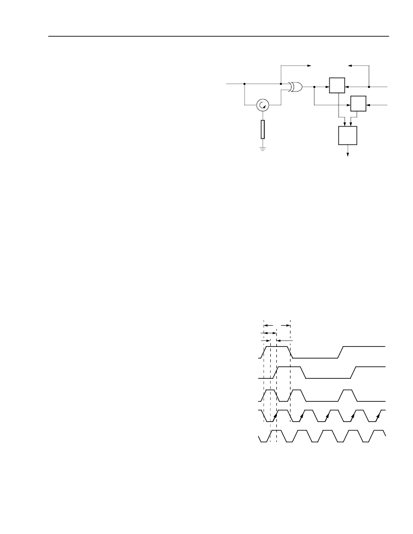
absent. The LG1600FXH features dual phase detec-
tors; one driven by an in-phase clock which is also driv-
ing the decision circuit flip-flop, the other is driven by a
quadrature clock. The phase detectors produce a zero
output when their respective clocks are centered with
respect to the transition pulses.
12-3226(F)r.3
Figure 3. Frequency and Phase Detector
For a transition pulse of half the width of the bit period,
the timing diagram of Figure 4 shows how the in-phase
clock ends up in the center of the data eye when the
quadrature-phase detector output is forced to zero by
the loop. The (patented) transition detector is com-
prised of an (active) circulator, a shorted stub, and an
exclusive-OR gate. The circulator/stub combination
produces a delayed version of the data. A transition at
the input of the circuit results in an output pulse from
the exclusive-OR gate whose width equals the return
delay of the stub. The stub is tuned for a given bit rate
and can be adjusted so that the in-phase clock is
exactly centered in the error-free phase range of the
retiming flip-flop.
12-3227(F)r.2
Figure 4. Timing Diagram
PDQ
PDI
LOGIC
TO FLIP-FLOP
FROM
VCO
90
°
0
°
TRANSITION
PULSE
DATA
CIRCULATOR
DELAYED
DATA
STUB
FPD OUT
90
°
0
°
TRANSITION
PULSE
DELAYED
DATA
DATA
1/2 T
1/4 T
CLOCK
CLOCK
T
相關(guān)PDF資料 |
PDF描述 |
|---|---|
| TF1006A | LG1625AXF Laser Driver |
| TFA9841J | 1-channel audio amplifier |
| TFA9843J | 2-channel audio amplifier (SE: 1 W to 20 W or BTL: 4 W to 40 W) |
| TFDS3000 | CONNECTOR ACCESSORY |
| TFMS5560 | Photo Modules for PCM Remote Control Systems |
相關(guān)代理商/技術(shù)參數(shù) |
參數(shù)描述 |
|---|---|
| TF100-5 | 制造商:RHOMBUS-IND 制造商全稱:Rhombus Industries Inc. 功能描述:TF Series High Performance 20 Section 10-Tap Delay Lines / SP3 Series |
| TF100505 | 制造商:FRONTIER 制造商全稱:Frontier Electronics. 功能描述:Tape and Reel Specifications |
| TF100505-10NJ | 制造商:FRONTIER 制造商全稱:Frontier Electronics. 功能描述:Multi-layers Chip Inductors |
| TF100505-10NK | 制造商:FRONTIER 制造商全稱:Frontier Electronics. 功能描述:Multi-layers Chip Inductors |
| TF100505-12NJ | 制造商:FRONTIER 制造商全稱:Frontier Electronics. 功能描述:Multi-layers Chip Inductors |
發(fā)布緊急采購(gòu),3分鐘左右您將得到回復(fù)。