- 您現(xiàn)在的位置:買賣IC網(wǎng) > PDF目錄98220 > THS3001CDGNRG4 (TEXAS INSTRUMENTS INC) 1 CHANNEL, VIDEO AMPLIFIER, PDSO8 PDF資料下載
參數(shù)資料
| 型號(hào): | THS3001CDGNRG4 |
| 廠商: | TEXAS INSTRUMENTS INC |
| 元件分類: | 音頻/視頻放大 |
| 英文描述: | 1 CHANNEL, VIDEO AMPLIFIER, PDSO8 |
| 封裝: | GREEN, PLASTIC, MSOP-8 |
| 文件頁(yè)數(shù): | 12/38頁(yè) |
| 文件大?。?/td> | 875K |
| 代理商: | THS3001CDGNRG4 |
第1頁(yè)第2頁(yè)第3頁(yè)第4頁(yè)第5頁(yè)第6頁(yè)第7頁(yè)第8頁(yè)第9頁(yè)第10頁(yè)第11頁(yè)當(dāng)前第12頁(yè)第13頁(yè)第14頁(yè)第15頁(yè)第16頁(yè)第17頁(yè)第18頁(yè)第19頁(yè)第20頁(yè)第21頁(yè)第22頁(yè)第23頁(yè)第24頁(yè)第25頁(yè)第26頁(yè)第27頁(yè)第28頁(yè)第29頁(yè)第30頁(yè)第31頁(yè)第32頁(yè)第33頁(yè)第34頁(yè)第35頁(yè)第36頁(yè)第37頁(yè)第38頁(yè)

SLOS217H – JULY 1998 – REVISED SEPTEMBER 2009................................................................................................................................................. www.ti.com
This integrated circuit can be damaged by ESD. Texas Instruments recommends that all integrated circuits be handled with
appropriate precautions. Failure to observe proper handling and installation procedures can cause damage.
ESD damage can range from subtle performance degradation to complete device failure. Precision integrated circuits may be more
susceptible to damage because very small parametric changes could cause the device not to meet its published specifications.
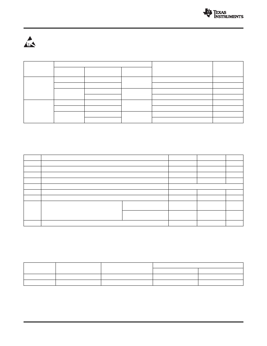
AVAILABLE OPTIONS(1)
PACKAGED DEVICE
TRANSPORT MEDIA,
EVALUATION
TA
SOIC
MSOP
QUANTITY
MODULE
(D)
(DGN)
SYMBOL
THS3001CD
THS3001CDGN
Rails, 75
ADP
THS3001CDR
THS3001CDGNR
Tape and Reel, 2500
--
0°C to 70°C
THS3001HVCDGN
Rails, 75
--
BNK
THS3001HVCDGNR
Tape and Reel, 2500
--
THS3001ID
THS3001IDGN
Rails, 75
--
ADQ
THS3001IDR
THS3001IDGNR
Tape and Reel, 2500
--
-40°C to 85°C
THS3001HVIDGN
Rails, 75
--
BNJ
THS3001HVIDGNR
Tape and Reel, 2500
--
(1)
For the most current package and ordering information, see the Package Option Addendum at the end of this document, or see the TI
website at www.ti.com.
ABSOLUTE MAXIMUM RATINGS
(1)
over operating free-air temperature range (unless otherwise noted)
THS3001
THS3001HV
UNITS
VSS
Supply voltage, VCC+ to VCC-
33
37
V
VI
Input voltage
±VCC
V
IO
Output current
175
mA
VID
Differential input voltage
±6
V
Continuous total power dissipation
See Dissipation Rating Table
TJ
Maximum junction temperature (2)
150
°C
TJ
Maximum junction temperature, continuous operation, long term reliability(3)
125
°C
THS3001C,
0 to 70
°C
THS3001HVC
TA
Operating free-air temperature
THS3001I,
–40 to 85
°C
THS3001HVI
Tstg
Storage temperature
–65 to 125
°C
(1)
Stresses above these ratings may cause permanent damage. Exposure to absolute maximum conditions for extended periods may
degrade device reliability. These are stress ratings only, and functional operation of the device at these or any other conditions beyond
those specified is not implied.
(2)
The absolute maximum temperature under any condition is limited by the constraints of the silicon process.
(3)
The maximum junction temperature for continuous operation is limited by package constraints. Operation above this temperature may
result in reduced reliability and/or lifetime of the device.
DISSIPATION RATING TABLE
POWER RATING (2)
θJC
θJA
(1)
PACKAGE
(°C/W)
TA ≤ 25°C
TA = 85°C
D (8)
38.3
97.5
1.02 W
410 mW
DGN (8)
4.7
58.4
1.71 W
685 mW
(1)
This data was taken using the JEDEC standard High-K test PCB.
(2)
Power rating is determined with a junction temperature of 125°C. This is the point where distortion starts to substantially increase.
Thermal management of the final PCB should strive to keep the junction temperature at or below 125°C for best performance and long
term reliability.
2
Copyright 1998–2009, Texas Instruments Incorporated
Product Folder Link(s): THS3001
相關(guān)PDF資料 |
PDF描述 |
|---|---|
| THS3001HVCDGN | 1 CHANNEL, VIDEO AMPLIFIER, PDSO8 |
| THS3001HVIDGNR | 1 CHANNEL, VIDEO AMPLIFIER, PDSO8 |
| THS3001HVIDGN | 1 CHANNEL, VIDEO AMPLIFIER, PDSO8 |
| THS3001IDGNG4 | 1 CHANNEL, VIDEO AMPLIFIER, PDSO8 |
| THS3001IDGNRG4 | 1 CHANNEL, VIDEO AMPLIFIER, PDSO8 |
相關(guān)代理商/技術(shù)參數(shù) |
參數(shù)描述 |
|---|---|
| THS3001CDR | 功能描述:高速運(yùn)算放大器 420-MHz Curr Feedback Amp RoHS:否 制造商:Texas Instruments 通道數(shù)量:1 電壓增益 dB:116 dB 輸入補(bǔ)償電壓:0.5 mV 轉(zhuǎn)換速度:55 V/us 工作電源電壓:36 V 電源電流:7.5 mA 最大工作溫度:+ 85 C 安裝風(fēng)格:SMD/SMT 封裝 / 箱體:SOIC-8 封裝:Tube |
| THS3001CDRG4 | 功能描述:高速運(yùn)算放大器 420-MHz Curr Feedback Amp RoHS:否 制造商:Texas Instruments 通道數(shù)量:1 電壓增益 dB:116 dB 輸入補(bǔ)償電壓:0.5 mV 轉(zhuǎn)換速度:55 V/us 工作電源電壓:36 V 電源電流:7.5 mA 最大工作溫度:+ 85 C 安裝風(fēng)格:SMD/SMT 封裝 / 箱體:SOIC-8 封裝:Tube |
| THS3001D | 制造商:TI 制造商全稱:Texas Instruments 功能描述:420-MHz HIGH-SPEED CURRENT-FEEDBACK AMPLIFIERS |
| THS3001DGN | 制造商:TI 制造商全稱:Texas Instruments 功能描述:420-MHz HIGH-SPEED CURRENT-FEEDBACK AMPLIFIERS |
| THS3001-DIE | 制造商:TI 制造商全稱:Texas Instruments 功能描述:420-MHz HIGH-SPEED CURRENT-FEEDBACK AMPLIFIER |
發(fā)布緊急采購(gòu),3分鐘左右您將得到回復(fù)。