- 您現(xiàn)在的位置:買賣IC網(wǎng) > PDF目錄67344 > THS4062CDGN (TEXAS INSTRUMENTS INC) 1 CHANNEL, VIDEO AMPLIFIER, PDSO8 PDF資料下載
參數(shù)資料
| 型號: | THS4062CDGN |
| 廠商: | TEXAS INSTRUMENTS INC |
| 元件分類: | 音頻/視頻放大 |
| 英文描述: | 1 CHANNEL, VIDEO AMPLIFIER, PDSO8 |
| 封裝: | GREEN, PLASTIC, MSOP-8 |
| 文件頁數(shù): | 9/31頁 |
| 文件大?。?/td> | 849K |
| 代理商: | THS4062CDGN |
第1頁第2頁第3頁第4頁第5頁第6頁第7頁第8頁當前第9頁第10頁第11頁第12頁第13頁第14頁第15頁第16頁第17頁第18頁第19頁第20頁第21頁第22頁第23頁第24頁第25頁第26頁第27頁第28頁第29頁第30頁第31頁

THS4061, THS4062
180MHz HIGHSPEED AMPLIFIERS
SLOS234E DECEMBER 1998 REVISED DECEMBER 2003
17
POST OFFICE BOX 655303
DALLAS, TEXAS 75265
APPLICATION INFORMATION
driving a capacitive load
Driving capacitive loads with high performance amplifiers is not a problem as long as certain precautions are
taken. The first is to realize that the THS406x has been internally compensated to maximize its bandwidth and
slew rate performance. When the amplifier is compensated in this manner, capacitive loading directly on the
output will decrease the device’s phase margin leading to high frequency ringing or oscillations. Therefore, for
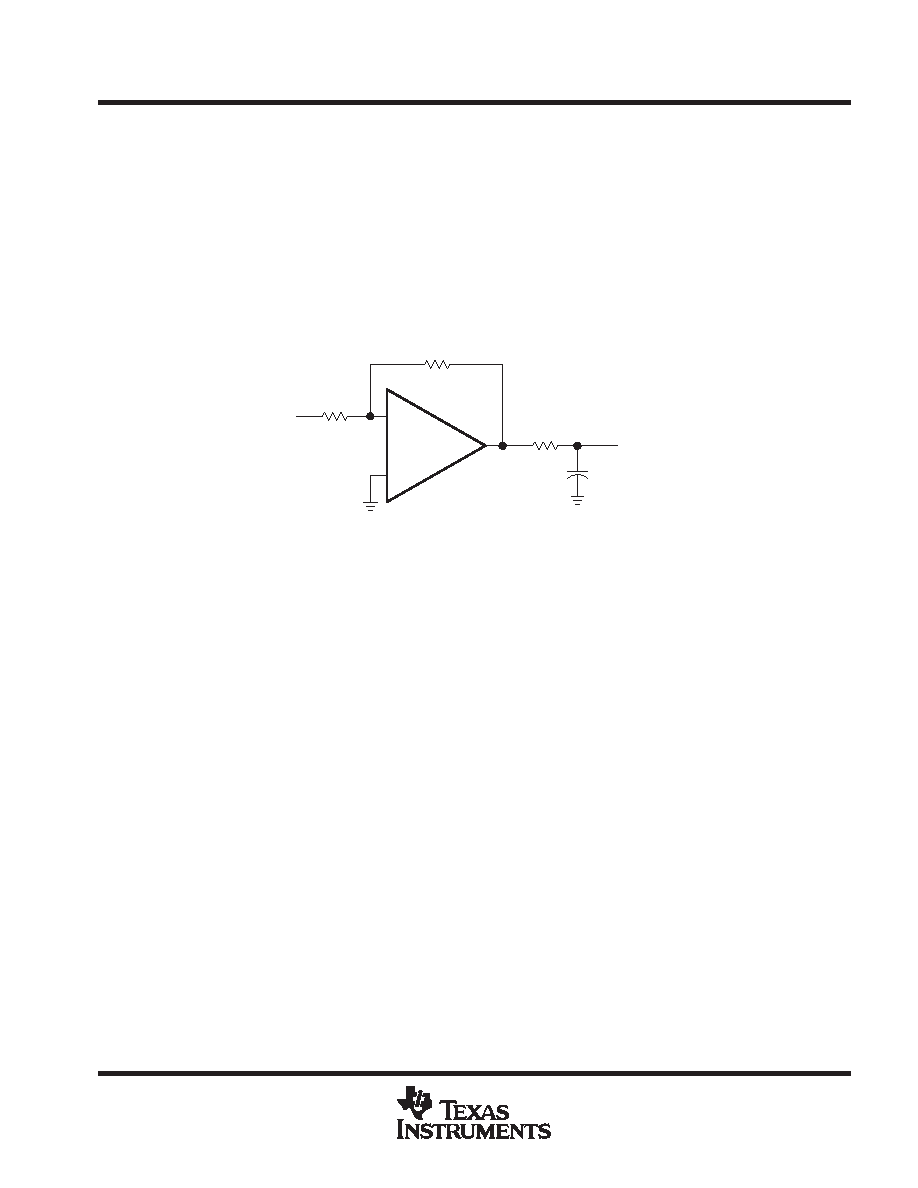
capacitive loads of greater than 10 pF, it is recommended that a resistor be placed in series with the output of
the amplifier, as shown in Figure 28. A minimum value of 20
should work well for most applications. For
example, in 75-
transmission systems, setting the series resistor value to 75 both isolates any capacitance
loading and provides the proper line impedance matching at the source end.
+
_
THS406x
CLOAD
510
Input
Output
510
20
Figure 28. Driving a Capacitive Load
circuit layout considerations
In order to achieve the levels of high frequency performance of the THS406x, it is essential that proper
printed-circuit board high frequency design techniques be followed. A general set of guidelines is given below.
In addition, a THS406x evaluation board is available to use as a guide for layout or for evaluating the device
performance.
D Ground planes It is highly recommended that a ground plane be used on the board to provide all
components with a low inductive ground connection. However, in the areas of the amplifier inputs and
output, the ground plane can be removed to minimize the stray capacitance.
D Proper power supply decoupling Use a 6.8-F tantalum capacitor in parallel with a 0.1-F ceramic
capacitor on each supply terminal. It may be possible to share the tantalum among several amplifiers
depending on the application, but a 0.1-
F ceramic capacitor should always be used on the supply terminal
of every amplifier. In addition, the 0.1-
F capacitor should be placed as close as possible to the supply
terminal. As this distances increases, the inductance in the connecting trace makes the capacitor less
effective. The designer should strive for distances of less than 0.1 inches between the device power
terminals and the ceramic capacitors.
D Sockets Sockets are not recommended for high-speed operational amplifiers. The additional lead
inductance in the socket pins will often lead to stability problems. Surface-mount packages soldered directly
to the printed-circuit board is the best implementation.
D Short trace runs/compact part placements Optimum high frequency performance is achieved when stray
series inductance has been minimized. To realize this, the circuit layout should be made as compact as
possible thereby minimizing the length of all trace runs. Particular attention should be paid to the inverting
input of the amplifier. Its length should be kept as short as possible. This helps to minimize stray capacitance
at the input of the amplifier.
相關PDF資料 |
PDF描述 |
|---|---|
| THS4062CDR | 1 CHANNEL, VIDEO AMPLIFIER, PDSO8 |
| THS4062CD | 1 CHANNEL, VIDEO AMPLIFIER, PDSO8 |
| THS4062IDGNR | 1 CHANNEL, VIDEO AMPLIFIER, PDSO8 |
| THS4062IDGN | 1 CHANNEL, VIDEO AMPLIFIER, PDSO8 |
| THS4062IDR | 1 CHANNEL, VIDEO AMPLIFIER, PDSO8 |
相關代理商/技術參數(shù) |
參數(shù)描述 |
|---|---|
| THS4062CDGNG4 | 功能描述:高速運算放大器 180-MHz High Output Drive RoHS:否 制造商:Texas Instruments 通道數(shù)量:1 電壓增益 dB:116 dB 輸入補償電壓:0.5 mV 轉換速度:55 V/us 工作電源電壓:36 V 電源電流:7.5 mA 最大工作溫度:+ 85 C 安裝風格:SMD/SMT 封裝 / 箱體:SOIC-8 封裝:Tube |
| THS4062CDGNR | 功能描述:高速運算放大器 180-MHz High Output Drive RoHS:否 制造商:Texas Instruments 通道數(shù)量:1 電壓增益 dB:116 dB 輸入補償電壓:0.5 mV 轉換速度:55 V/us 工作電源電壓:36 V 電源電流:7.5 mA 最大工作溫度:+ 85 C 安裝風格:SMD/SMT 封裝 / 箱體:SOIC-8 封裝:Tube |
| THS4062CDGNRG4 | 功能描述:高速運算放大器 180-MHz High Output Drive RoHS:否 制造商:Texas Instruments 通道數(shù)量:1 電壓增益 dB:116 dB 輸入補償電壓:0.5 mV 轉換速度:55 V/us 工作電源電壓:36 V 電源電流:7.5 mA 最大工作溫度:+ 85 C 安裝風格:SMD/SMT 封裝 / 箱體:SOIC-8 封裝:Tube |
| THS4062CDR | 功能描述:高速運算放大器 180-MHz High Output Drive RoHS:否 制造商:Texas Instruments 通道數(shù)量:1 電壓增益 dB:116 dB 輸入補償電壓:0.5 mV 轉換速度:55 V/us 工作電源電壓:36 V 電源電流:7.5 mA 最大工作溫度:+ 85 C 安裝風格:SMD/SMT 封裝 / 箱體:SOIC-8 封裝:Tube |
| THS4062CDRG4 | 功能描述:高速運算放大器 180-MHz High Output Drive RoHS:否 制造商:Texas Instruments 通道數(shù)量:1 電壓增益 dB:116 dB 輸入補償電壓:0.5 mV 轉換速度:55 V/us 工作電源電壓:36 V 電源電流:7.5 mA 最大工作溫度:+ 85 C 安裝風格:SMD/SMT 封裝 / 箱體:SOIC-8 封裝:Tube |
發(fā)布緊急采購,3分鐘左右您將得到回復。