- 您現(xiàn)在的位置:買賣IC網(wǎng) > PDF目錄98229 > THS7375IPWR (TEXAS INSTRUMENTS INC) VIDEO AMPLIFIER, PDSO14 PDF資料下載
參數(shù)資料
| 型號: | THS7375IPWR |
| 廠商: | TEXAS INSTRUMENTS INC |
| 元件分類: | 音頻/視頻放大 |
| 英文描述: | VIDEO AMPLIFIER, PDSO14 |
| 封裝: | GREEN, PLASTIC, TSSOP-14 |
| 文件頁數(shù): | 11/39頁 |
| 文件大小: | 973K |
| 代理商: | THS7375IPWR |
第1頁第2頁第3頁第4頁第5頁第6頁第7頁第8頁第9頁第10頁當前第11頁第12頁第13頁第14頁第15頁第16頁第17頁第18頁第19頁第20頁第21頁第22頁第23頁第24頁第25頁第26頁第27頁第28頁第29頁第30頁第31頁第32頁第33頁第34頁第35頁第36頁第37頁第38頁第39頁

+V
S
External
Input/Output
Pin
Internal
Circuitry
www.ti.com
SBOS449A – SEPTEMBER 2008 – REVISED JANUARY 2011
APPLICATION INFORMATION
Place a 0.1-mF to 0.01-mF capacitor as close as
The THS7375 is targeted for standard definition video
possible to the power-supply pins. Failure to do so
output buffer applications. Although it can be used for
may result in ringing or oscillating at the THS7375
numerous
other
applications,
the
needs
and
outputs. Additionally, a large capacitor (22 mF to 100
requirements of the video signal are the most
mF) should be placed on the power-supply line to
important design parameters of the THS7375. Built
minimize
interference
with
50-Hz/60-Hz
line
on
the
revolutionary
complementary
Silicon
frequencies.
Germanium (SiGe) BiCom3X process, the THS7375
incorporates many features not typically found in
INPUT VOLTAGE
integrated video parts while consuming very low
power. The THS7375 has the following features:
The THS7375 input range allows for an input signal
range from –0.2 V to approximately (VS+ – 1.5 V).
Single-supply 3-V to 5-V operation with low total
However, because of the internal fixed gain of 5.6
quiescent current of 9.8 mA at 3.3 V and 10.3 mA
V/V (+14.95 dB) and the internal level shift that
at 5 V.
causes a 320-mV level shift, the output is generally
Disable mode allows for shutting down the
the limiting factor for the allowable linear input range.
THS7375
to
save
system
power
in
For example, with a 5-V supply, the linear input range
power-sensitive applications.
is from –0.2 V to 3.5 V. As a result of the gain and
Input configuration accepts dc + level shift, ac
level shift, the linear output range limits the allowable
sync-tip clamp, or ac-bias.
linear input range to be from about –0.1 V to 0.8 V.
AC-biasing is allowed with the use of a single
external pull-up resistor to the positive power
INPUT OVERVOLTAGE PROTECTION
supply.
The THS7375 is built using a very high-speed
Sixth-order low-pass filter for DAC reconstruction
complementary bipolar and CMOS process. The
or ADC image rejection:
internal junction breakdown voltages are relatively
–
9.5 MHz for NTSC, PAL, SECAM, composite
low for these very small geometry devices. These
(CVBS), S-Video Y’C’, 480i/576i Y’P’BP’R,
breakdowns are reflected in the Absolute Maximum
G’B’R’ (R'G'B'), and SCART signals.
Ratings table. All input and output device pins are
Bypass mode bypasses the low-pass filter with a
protected with internal ESD protection diodes to the
70-MHz
bandwidth
and
150-V/ms
slew
rate
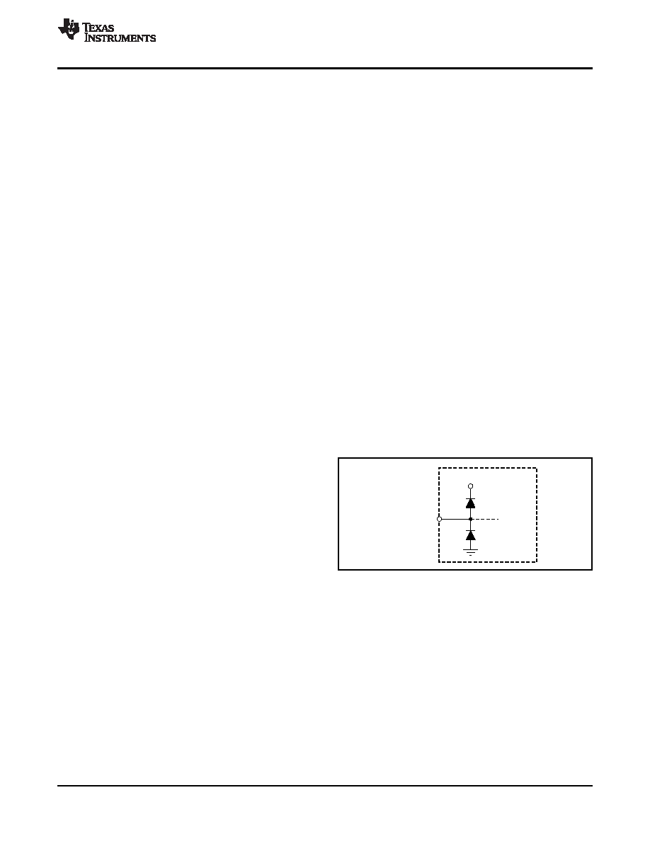
power supplies, as shown in Figure 47.
amplifier
Internal fixed gain of 5.6 V/V (+14.95 dB) buffer
that can drive two video lines per channel with
dc-coupling or traditional ac-coupling. This feature
is ideal for DaVinci, DM2xx, DM3xx, DM64xx, and
OMAP processors.
Signal flow-through configuration in a TSSOP-14
package that complies with the latest lead-free
(RoHS-compatible)
and
green
manufacturing
requirements.
Figure 47. Internal ESD Protection
OPERATING VOLTAGE
The THS7375 is designed to operate from 3-V to 5-V
These diodes provide moderate protection to input
over a –40°C to +85°C temperature range. The
overdrive voltages above and below the supplies as
impact on performance over the entire temperature
well. The protection diodes can typically support 30
range is negligible as a result of the implementation
mA of continuous current when overdriven.
of thin film resistors and high quality, low temperature
coefficient capacitors. The design of the THS7375
allows
operation
down
to
2.85
V,
but
it
is
recommended to use at least a 3-V supply to ensure
that there are no issues with headroom or clipping.
Copyright 2008–2011, Texas Instruments Incorporated
19
Product Folder Link(s): THS7375
相關(guān)PDF資料 |
PDF描述 |
|---|---|
| THS7375IPW | VIDEO AMPLIFIER, PDSO14 |
| THS7375IPWG4 | VIDEO AMPLIFIER, PDSO14 |
| THS7375IPWRG4 | VIDEO AMPLIFIER, PDSO14 |
| THS770012IRGET | SPECIALTY ANALOG CIRCUIT, PQCC24 |
| THS8083-95CPZP | SPECIALTY CONSUMER CIRCUIT, PQFP100 |
相關(guān)代理商/技術(shù)參數(shù) |
參數(shù)描述 |
|---|---|
| THS7375IPWRG4 | 功能描述:視頻放大器 4Ch SDTV Video Amp w/6th order fltr RoHS:否 制造商:ON Semiconductor 通道數(shù)量:4 電源類型: 工作電源電壓:3.3 V, 5 V 電源電流: 最小工作溫度: 最大工作溫度: 封裝 / 箱體:TSSOP-14 封裝:Reel |
| THS7376 | 制造商:TI 制造商全稱:Texas Instruments 功能描述:4-Channel Video Amplifier with One SD and Three HD 8th-Order Filters with 6-dB Gain |
| THS7376IPW | 制造商:Texas Instruments 功能描述:4-Channel Video Amplifier 1SD 3HD 制造商:Texas Instruments 功能描述:IC SDTV VIDEO AMP 4-CH 14-TSSOP |
| THS7376IPWR | 制造商:Texas Instruments 功能描述:4-Channel Video Amplifier 1SD 3HD |
| THS7380IZSYR | 制造商:Texas Instruments 功能描述: 制造商:Texas Instruments 功能描述:AMPLIFIER-NON VMI |
發(fā)布緊急采購,3分鐘左右您將得到回復。