- 您現(xiàn)在的位置:買賣IC網(wǎng) > PDF目錄98235 > TLC1542MJ (TEXAS INSTRUMENTS INC) 11-CH 10-BIT SUCCESSIVE APPROXIMATION ADC, SERIAL ACCESS, CDIP20 PDF資料下載
參數(shù)資料
| 型號: | TLC1542MJ |
| 廠商: | TEXAS INSTRUMENTS INC |
| 元件分類: | ADC |
| 英文描述: | 11-CH 10-BIT SUCCESSIVE APPROXIMATION ADC, SERIAL ACCESS, CDIP20 |
| 封裝: | CERAMIC, DIP-20 |
| 文件頁數(shù): | 1/25頁 |
| 文件大小: | 583K |
| 代理商: | TLC1542MJ |

TLC1542EP, TLC1543EP
10BIT ANALOGTODIGITAL CONVERTERS WITH
SERIAL CONTROL AND 11 ANALOG INPUTS
SGLS152A JANUARY 2004 REVISED FEBRUARY 2006
1
POST OFFICE BOX 655303
DALLAS, TEXAS 75265
D Controlled Baseline
One Assembly/Test Site, One Fabrication
Site
D Extended Temperature Performance of
40
°C to 125°C
D Enhanced Diminishing Manufacturing
Sources (DMS) Support
D Enhanced Product Change Notification
D Qualification Pedigree
D 10-Bit Resolution A/D Converter
D 11 Analog Input Channels
D Three Built-In Self-Test Modes
D Inherent Sample-and-Hold Function
D Total Unadjusted Error . . . ±1 LSB Max
D On-Chip System Clock
D End-of-Conversion (EOC) Output
D Terminal Compatible With TLC542
D CMOS Technology
description
The TLC1542-EP and TLC1543-EP are CMOS 10-bit switched-capacitor successive-approximation
analog-to-digital converters. These devices have three inputs, a 3-state output chip select (CS), input/output
clock (I/O CLOCK), address input (ADDRESS), and data output (DATA OUT)] that provide a direct 4-wire
interface to the serial port of a host processor. The TLC1542-EP and TLC1543-EP allow high-speed data
transfers from the host.
In addition to a high-speed A /D converter and versatile control capability, the TLC1542-EP and TLC1543-EP
have an on-chip 14-channel multiplexer that can select any one of 11 analog inputs or any one of three internal
self-test voltages. The sample-and-hold function is automatic. At the end of the A /D conversion, the
end-of-conversion (EOC) output goes high to indicate that conversion is complete. The converter incorporated
in the TLC1542-EP and TLC1543-EP features differential high-impedance reference inputs that facilitate
ratiometric conversion, scaling, and isolation of analog circuitry from logic and supply noise. A
switched-capacitor design allows low-error conversion over the full operating free-air temperature range.
Please be aware that an important notice concerning availability, standard warranty, and use in critical applications of
Texas Instruments semiconductor products and disclaimers thereto appears at the end of this data sheet.
Component qualification in accordance with JEDEC and industry standards to ensure reliable operation over an extended temperature range.
This includes, but is not limited to, Highly Accelerated Stress Test (HAST) or biased 85/85, temperature cycle, autoclave or unbiased HAST,
electromigration, bond intermetallic life, and mold compound life. Such qualification testing should not be viewed as justifying use of this
component beyond specified performance and environmental limits.
This document contains information on products in more than one phase
of development. The status of each device is indicated on the page(s)
specifying its electrical characteristics.
Copyright
2006, Texas Instruments Incorporated
1
2
3
4
5
6
7
8
9
10
20
19
18
17
16
15
14
13
12
11
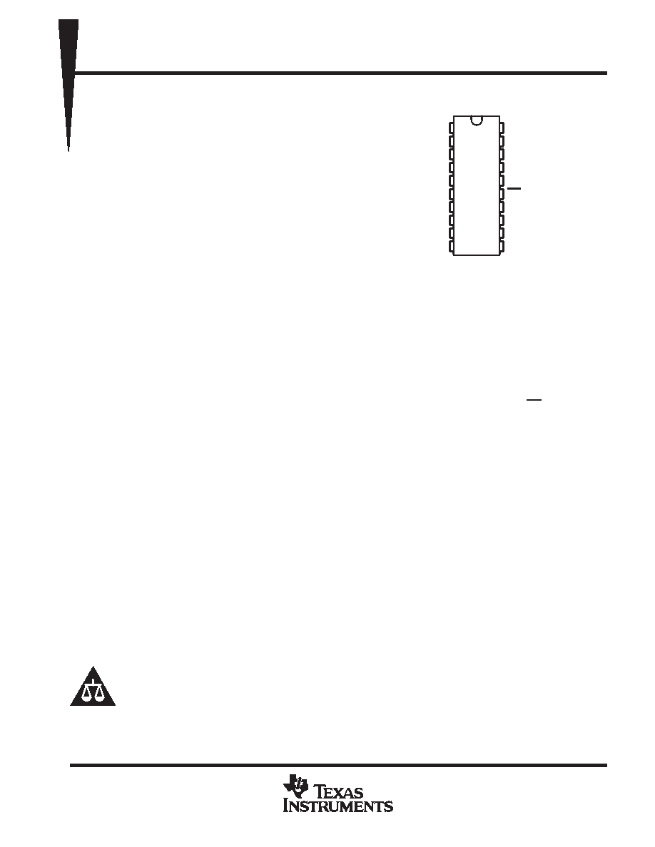
A0
A1
A2
A3
A4
A5
A6
A7
A8
GND
VCC
EOC
I/O CLOCK
ADDRESS
DATA OUT
CS
REF +
REF
A10
A9
DW PACKAGE
(TOP VIEW)
相關(guān)PDF資料 |
PDF描述 |
|---|---|
| TLC1542MFK | 11-CH 10-BIT SUCCESSIVE APPROXIMATION ADC, SERIAL ACCESS, CQCC20 |
| TLC1542QDWR | 11-CH 10-BIT SUCCESSIVE APPROXIMATION ADC, SERIAL ACCESS, PDSO20 |
| TLC1542QDB | 11-CH 10-BIT SUCCESSIVE APPROXIMATION ADC, SERIAL ACCESS, PDSO20 |
| TLC1542QN | 11-CH 10-BIT SUCCESSIVE APPROXIMATION ADC, SERIAL ACCESS, PDIP20 |
| TLC1542QDW | 11-CH 10-BIT SUCCESSIVE APPROXIMATION ADC, SERIAL ACCESS, PDSO20 |
相關(guān)代理商/技術(shù)參數(shù) |
參數(shù)描述 |
|---|---|
| TLC1542MJB | 制造商:TI 制造商全稱:Texas Instruments 功能描述:10-BIT ANALOG-TO-DIGITAL CONVERTERS WITH SERIAL CONTROL AND 11 ANALOG INPUTS |
| TLC1542Q | 制造商:TI 制造商全稱:Texas Instruments 功能描述:10-BIT ANALOG-TO-DIGITAL CONVERTERS WITH SERIAL CONTROL AND 11 ANALOG INPUTS |
| TLC1542QDB | 制造商:TI 制造商全稱:Texas Instruments 功能描述:10-BIT ANALOG-TO-DIGITAL CONVERTERS WITH SERIAL CONTROL AND 11 ANALOG INPUTS |
| TLC1542QDW | 制造商:TI 制造商全稱:Texas Instruments 功能描述:10-BIT ANALOG-TO-DIGITAL CONVERTERS WITH SERIAL CONTROL AND 11 ANALOG INPUTS |
| TLC1542QFN | 功能描述:模數(shù)轉(zhuǎn)換器 - ADC 10bit 11Chl A/D RoHS:否 制造商:Texas Instruments 通道數(shù)量:2 結(jié)構(gòu):Sigma-Delta 轉(zhuǎn)換速率:125 SPs to 8 KSPs 分辨率:24 bit 輸入類型:Differential 信噪比:107 dB 接口類型:SPI 工作電源電壓:1.7 V to 3.6 V, 2.7 V to 5.25 V 最大工作溫度:+ 85 C 安裝風(fēng)格:SMD/SMT 封裝 / 箱體:VQFN-32 |
發(fā)布緊急采購,3分鐘左右您將得到回復(fù)。