- 您現(xiàn)在的位置:買賣IC網(wǎng) > PDF目錄98235 > TLC1550MJB (TEXAS INSTRUMENTS INC) 1-CH 10-BIT SUCCESSIVE APPROXIMATION ADC, PARALLEL ACCESS, CDIP24 PDF資料下載
參數(shù)資料
| 型號: | TLC1550MJB |
| 廠商: | TEXAS INSTRUMENTS INC |
| 元件分類: | ADC |
| 英文描述: | 1-CH 10-BIT SUCCESSIVE APPROXIMATION ADC, PARALLEL ACCESS, CDIP24 |
| 封裝: | CERAMIC, DIP-24 |
| 文件頁數(shù): | 13/16頁 |
| 文件大小: | 309K |
| 代理商: | TLC1550MJB |

TLC1550I, TLC1550M, TLC1551I
10BIT ANALOGTODIGITAL CONVERTERS
WITH PARALLEL OUTPUTS
SLAS043G MAY 1991 REVISED NOVEMBER 2003
6
POST OFFICE BOX 655303
DALLAS, TEXAS 75265
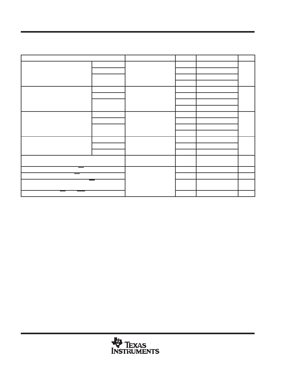
operating characteristics over recommended operating free-air temperature range with internal
clock and minimum sampling time of 4
s, VDD =VREF+ = 5 V and VREF = 0 (unless otherwise
noted)
PARAMETER
TEST CONDITIONS
TA
MIN
TYP
MAX
UNIT
TLC1550I
Full range
±0.5
EL
Linearity error
TLC1551I
See Note 3
Full range
±1
LSB
EL
Linearity error
TLC1550M
See Note 3
25
°C
±0.5
LSB
TLC1550M
Full range
±1
TLC1550I
Full range
±0.5
EZS
Zero-scale error
TLC1551I
See Notes 2 and 4
Full range
±1
LSB
EZS
Zero-scale error
TLC1550M
See Notes 2 and 4
25
°C
±0.5
LSB
TLC1550M
Full range
±1
TLC1550I
Full range
±0.5
EFS
Full-scale error
TLC1551I
See Notes 2 and 4
Full range
±1
LSB
EFS
Full-scale error
TLC1550M
See Notes 2 and 4
25
°C
±0.5
LSB
TLC1550M
Full range
±1
TLC1550I
Full range
±0.5
Total unadjusted error
TLC1551I
See Note 5
Full range
±1
LSB
Total unadjusted error
TLC1550M
See Note 5
25
°C
±1
LSB
tc
Conversion time
fclock(external) = 4.2 MHz or
internal clock
6
s
ta(D)
Data access time after RD goes low
35
ns
tv(D)
Data valid time after RD goes high
5
ns
tdis(D)
Disable time, delay time from RD high to high
impedance
See Figure 3
30
ns
td(EOC) Delay time, RD low to EOC high
0
15
ns
Full range is 40°C to 85°C for the TL155xI devices and 55°C to 125°C for the TLC1550M.
All typical values are at VDD = 5 V, TA = 25°C.
NOTES:
2. Analog input voltages greater than that applied to REF+ convert to all 1s (1111111111), while input voltages less than that applied
to REF convert to all 0s (0000000000). The total unadjusted error may increase as this differential voltage falls below 4.75 V.
3. Linearity error is the difference between the actual analog value at the transition between any two adjacent steps and its ideal value
after zero-scale error and full-scale error have been removed.
4. Zero-scale error is the difference between the actual mid-step value and the nominal mid-step value at specified zero scale.
Full-scale error is the difference between the actual mid-step value and the nominal mid-step value at specified full scale.
5. Total unadjusted error is the difference between the actual analog value at the transition between any two adjacent steps and its
ideal value. It includes contributions from zero-scale error, full-scale error, and linearity error.
相關(guān)PDF資料 |
PDF描述 |
|---|---|
| TLC1550IDWRG4 | 1-CH 10-BIT SUCCESSIVE APPROXIMATION ADC, PARALLEL ACCESS, PDSO24 |
| TLC1550IDWG4 | 1-CH 10-BIT SUCCESSIVE APPROXIMATION ADC, PARALLEL ACCESS, PDSO24 |
| TLC1550IDW | 1-CH 10-BIT SUCCESSIVE APPROXIMATION ADC, PARALLEL ACCESS, PDSO24 |
| TLC1550MFK | 1-CH 10-BIT SUCCESSIVE APPROXIMATION ADC, PARALLEL ACCESS, CQCC28 |
| TLC1551IDWRG4 | 1-CH 10-BIT SUCCESSIVE APPROXIMATION ADC, PARALLEL ACCESS, PDSO24 |
相關(guān)代理商/技術(shù)參數(shù) |
參數(shù)描述 |
|---|---|
| TLC1550MNW | 制造商:TI 制造商全稱:Texas Instruments 功能描述:10-BIT ANALOG-TO-DIGITAL CONVERTERS WITH PARALLEL OUTPUTS |
| TLC1551DW | 制造商:Texas Instruments 功能描述: |
| TLC1551I | 制造商:TI 制造商全稱:Texas Instruments 功能描述:10-BIT ANALOG-TO-DIGITAL CONVERTERS WITH PARALLEL OUTPUTS |
| TLC1551IDW | 功能描述:模數(shù)轉(zhuǎn)換器 - ADC LiN-EPIC 10bit A/D RoHS:否 制造商:Texas Instruments 通道數(shù)量:2 結(jié)構(gòu):Sigma-Delta 轉(zhuǎn)換速率:125 SPs to 8 KSPs 分辨率:24 bit 輸入類型:Differential 信噪比:107 dB 接口類型:SPI 工作電源電壓:1.7 V to 3.6 V, 2.7 V to 5.25 V 最大工作溫度:+ 85 C 安裝風(fēng)格:SMD/SMT 封裝 / 箱體:VQFN-32 |
| TLC1551IDWG4 | 功能描述:模數(shù)轉(zhuǎn)換器 - ADC 10B 164kSPS ADC 10Ch RoHS:否 制造商:Texas Instruments 通道數(shù)量:2 結(jié)構(gòu):Sigma-Delta 轉(zhuǎn)換速率:125 SPs to 8 KSPs 分辨率:24 bit 輸入類型:Differential 信噪比:107 dB 接口類型:SPI 工作電源電壓:1.7 V to 3.6 V, 2.7 V to 5.25 V 最大工作溫度:+ 85 C 安裝風(fēng)格:SMD/SMT 封裝 / 箱體:VQFN-32 |
發(fā)布緊急采購,3分鐘左右您將得到回復(fù)。