- 您現在的位置:買賣IC網 > PDF目錄67343 > TLC5618ID (TEXAS INSTRUMENTS INC) SERIAL INPUT LOADING, 12.5 us SETTLING TIME, 12-BIT DAC, PDSO8 PDF資料下載
參數資料
| 型號: | TLC5618ID |
| 廠商: | TEXAS INSTRUMENTS INC |
| 元件分類: | DAC |
| 英文描述: | SERIAL INPUT LOADING, 12.5 us SETTLING TIME, 12-BIT DAC, PDSO8 |
| 封裝: | PLASTIC, SOIC-8 |
| 文件頁數: | 20/24頁 |
| 文件大?。?/td> | 480K |
| 代理商: | TLC5618ID |
TLC5618, TLC5618A
PROGRAMMABLE DUAL 12-BIT DIGITAL-TO-ANALOG CONVERTERS
SLAS156G – JULY 1997 – REVISED APRIL 2001
5
POST OFFICE BOX 655303
DALLAS, TEXAS 75265
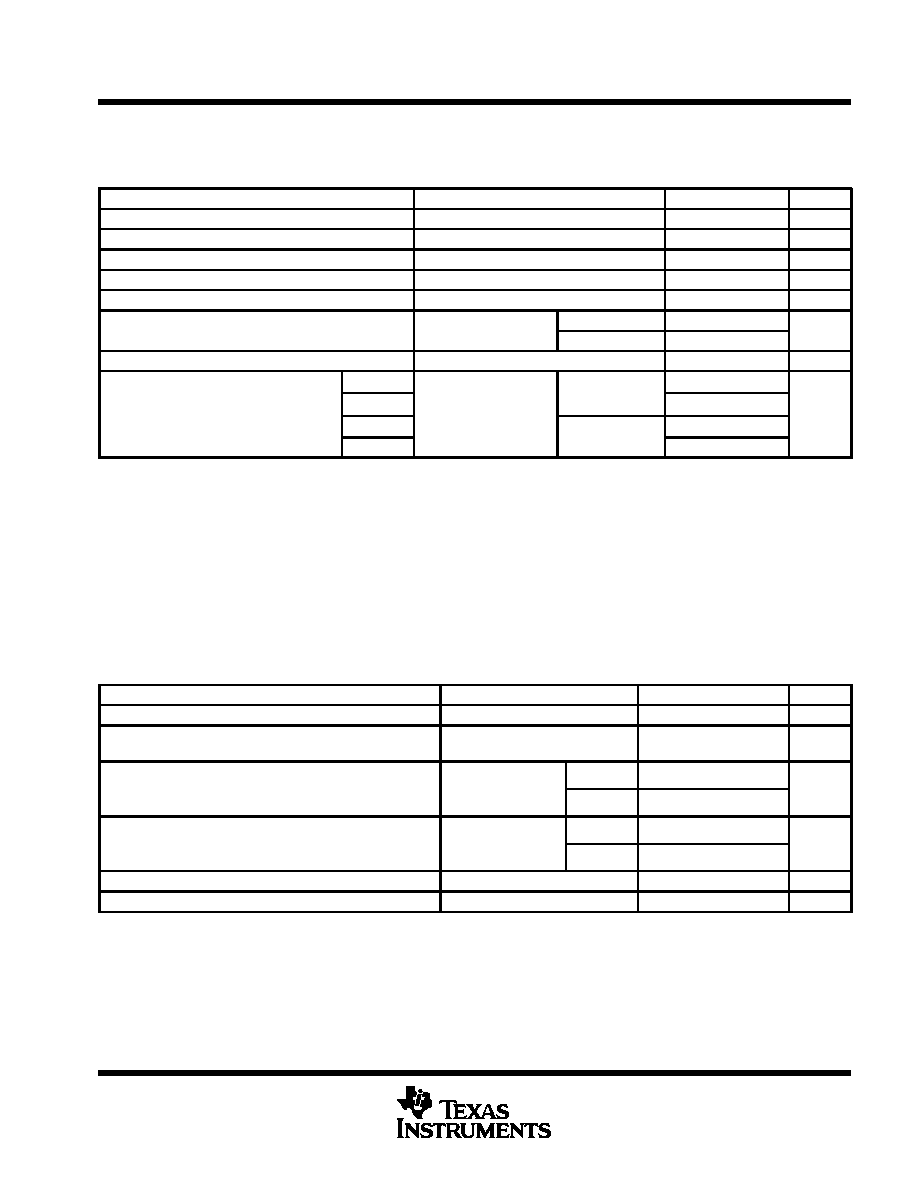
electrical characteristics over recommended operating free-air temperature range, VDD = 5 V ± 5%,
Vref(REFIN) = 2.048 V (unless otherwise noted)
static DAC specifications
PARAMETER
TEST CONDITIONS
MIN
TYP
MAX
UNIT
Resolution
12
bits
Integral nonlinearity (INL), end point adjusted
Vref(REFIN) = 2.048 V,
See Note 1
±4
LSB
Differential nonlinearity (DNL)
Vref(REFIN) = 2.048 V,
See Note 2
±0.5
± 1
LSB
EZS
Zero-scale error (offset error at zero scale)
Vref(REFIN) = 2.048 V,
See Note 3
±12
mV
Zero-scale-error temperature coefficient
Vref(REFIN) = 2.048 V,
See Note 4
3
ppm/
°C
EG
Gain error
Vref(REFIN) = 2.048 V,
C and I suffixes
±0.29 % of FS
EG
Gain error
ref(REFIN)
,
See Note 5
Q and M suffixes
±0.60
voltage
Gain error temperature coefficient
Vref(REFIN) = 2.048 V,
See Note 6
1
ppm/
°C
Zero scale
Slow
65
PSRR
Power-supply rejection ratio
Gain
See Notes 7 and 8
Slow
65
dB
PSRR
Power-su
ly rejection ratio
Zero scale
See Notes 7 and 8
Fast
65
dB
Gain
Fast
65
NOTES:
1. The relative accuracy or integral nonlinearity (INL) sometimes referred to as linearity error, is the maximum deviation of the output
from the line between zero and full scale excluding the effects of zero code and full-scale errors.
2. The differential nonlinearity (DNL) sometimes referred to as differential error, is the difference between the measured and ideal
1 LSB amplitude change of any two adjacent codes. Monotonic means the output voltage changes in the same direction (or remains
constant) as a change in the digital input code.
3. Zero-scale error is the deviation from zero voltage output when the digital input code is zero.
4. Zero-scale-error temperature coefficient is given by: EZS TC = [EZS (Tmax) – EZS (Tmin)]/Vref × 106/(Tmax – Tmin).
5. Gain error is the deviation from the ideal output (Vref – 1 LSB) with an output load of 10 k excluding the effects of the zero-error.
6. Gain temperature coefficient is given by: EG TC = [EG(Tmax) – EG (Tmin)]/Vref × 106/(Tmax – Tmin).
7. Zero-scale-error rejection ratio (EZS-RR) is measured by varying the VDD from 4.5 V to 5.5 V dc and measuring the proportion of
this signal imposed on the zero-code output voltage.
8. Gain-error rejection ratio (EG-RR) is measured by varying the VDD from 4.5 V to 5.5 V dc and measuring the proportion of this signal
imposed on the full-scale output voltage after subtracting the zero scale change.
OUT A and OUT B output specifications
PARAMETER
TEST CONDITIONS
MIN
TYP
MAX
UNIT
VO
Voltage output range
RL = 10 k
0
VDD–0.4
V
Output load regulation accuracy
VO(OUT) = 4.096 V,
RL = 2 k
±0.29
% of FS
voltage
IOSC(sink)
Output short circuit sink current
VO(A OUT) = VDD,
VO(B OUT) =VDD
Fast
38
mA
IOSC(sink)
Out ut short circuit sink current
VO(B OUT) = VDD,
Input code zero
Slow
23
mA
IOSC(source)
Output short circuit source current
VO(A OUT) = 0 V,
VO(B OUT) =0V
Fast
–54
mA
IOSC(source)
Out ut short circuit source current
VO(B OUT) = 0 V,
Full-scale code
Slow
–29
mA
IO(sink)
Output sink current
VO(OUT) = 0.25 V
5
mA
IO(source)
Output source current
VO(OUT) = 4.2 V
5
mA
相關PDF資料 |
PDF描述 |
|---|---|
| 5962-9957001Q2A | 8-CH 12-BIT SUCCESSIVE APPROXIMATION ADC, SERIAL ACCESS, CQCC20 |
| TLV2548MFKB | 8-CH 12-BIT SUCCESSIVE APPROXIMATION ADC, SERIAL ACCESS, CQCC20 |
| TLV2548QDWR | 8-CH 12-BIT SUCCESSIVE APPROXIMATION ADC, SERIAL ACCESS, PDSO20 |
| TLV2548QDW | 8-CH 12-BIT SUCCESSIVE APPROXIMATION ADC, SERIAL ACCESS, PDSO20 |
| TLV2544QDR | 4-CH 12-BIT SUCCESSIVE APPROXIMATION ADC, SERIAL ACCESS, PDSO16 |
相關代理商/技術參數 |
參數描述 |
|---|---|
| TLC5618IDR | 制造商:TI 制造商全稱:Texas Instruments 功能描述:PROGRAMMABLE DUAL 12-BIT DIGITAL-TO-ANALOG CONVERTERS |
| TLC5618IP | 制造商:TI 制造商全稱:Texas Instruments 功能描述:PROGRAMMABLE DUAL 12-BIT DIGITAL-TO-ANALOG CONVERTERS |
| TLC5620 | 制造商:TI 制造商全稱:Texas Instruments 功能描述:QUADRUPLE 8-BIT DIGITAL-TO-ANALOG CONVERTERS |
| TLC5620C | 制造商:TI 制造商全稱:Texas Instruments 功能描述:QUADRUPLE 8-BIT DIGITAL-TO-ANALOG CONVERTERS |
| TLC5620CD | 功能描述:數模轉換器- DAC Quad 8bit DigitAL/AN RoHS:否 制造商:Texas Instruments 轉換器數量:1 DAC 輸出端數量:1 轉換速率:2 MSPs 分辨率:16 bit 接口類型:QSPI, SPI, Serial (3-Wire, Microwire) 穩(wěn)定時間:1 us 最大工作溫度:+ 85 C 安裝風格:SMD/SMT 封裝 / 箱體:SOIC-14 封裝:Tube |
發(fā)布緊急采購,3分鐘左右您將得到回復。
