- 您現(xiàn)在的位置:買賣IC網(wǎng) > PDF目錄98252 > TLV2553IDW (TEXAS INSTRUMENTS INC) 11-CH 12-BIT SUCCESSIVE APPROXIMATION ADC, SERIAL ACCESS, PDSO20 PDF資料下載
參數(shù)資料
| 型號: | TLV2553IDW |
| 廠商: | TEXAS INSTRUMENTS INC |
| 元件分類: | ADC |
| 英文描述: | 11-CH 12-BIT SUCCESSIVE APPROXIMATION ADC, SERIAL ACCESS, PDSO20 |
| 封裝: | GREEN, PLASTIC, SOIC-20 |
| 文件頁數(shù): | 14/29頁 |
| 文件大小: | 603K |
| 代理商: | TLV2553IDW |
第1頁第2頁第3頁第4頁第5頁第6頁第7頁第8頁第9頁第10頁第11頁第12頁第13頁當前第14頁第15頁第16頁第17頁第18頁第19頁第20頁第21頁第22頁第23頁第24頁第25頁第26頁第27頁第28頁第29頁

TLV2553
SLAS354B – SEPTEMBER 2001 – REVISED SEPTEMBER 2002
21
www.ti.com
PRINCIPLES OF OPERATION
conversion cycle
A conversion cycle is started only after the I/O cycle is completed, which minimizes the influence of external
digital noise on the accuracy of the conversion. This cycle is transparent to the user because it is controlled by
an internal clock (oscillator). The total conversion time is equal to 13.5 OSC clocks plus a small delay (~25 ns)
to start the OSC. During the conversion period, the device performs a successive-approximation conversion
on the analog input voltage.
EOC goes low at the start of the conversion cycle and goes high when the conversion is complete and the output
data register is latched. After EOC goes low, the analog input can be changed without affecting the conversion
result. Since the delay from the falling edge of the last I/O CLOCK to the falling edge of EOC is fixed, any
time-varying analog input signals can be digitized at a fixed rate without introducing systematic harmonic
distortion or noise due to timing uncertainty.
power up and initialization
After power up, CS must be taken from high to low to begin an I/O cycle. The EOC pin is initially high, and the
configuration register is set to all zeroes. The contents of the output data register are random, and the first
conversion result should be ignored. To initialize during operation, CS is taken high and is then returned low
to begin the next I/O cycle. The first conversion after the device has returned from the power-down state may
not read accurately due to internal device settling.
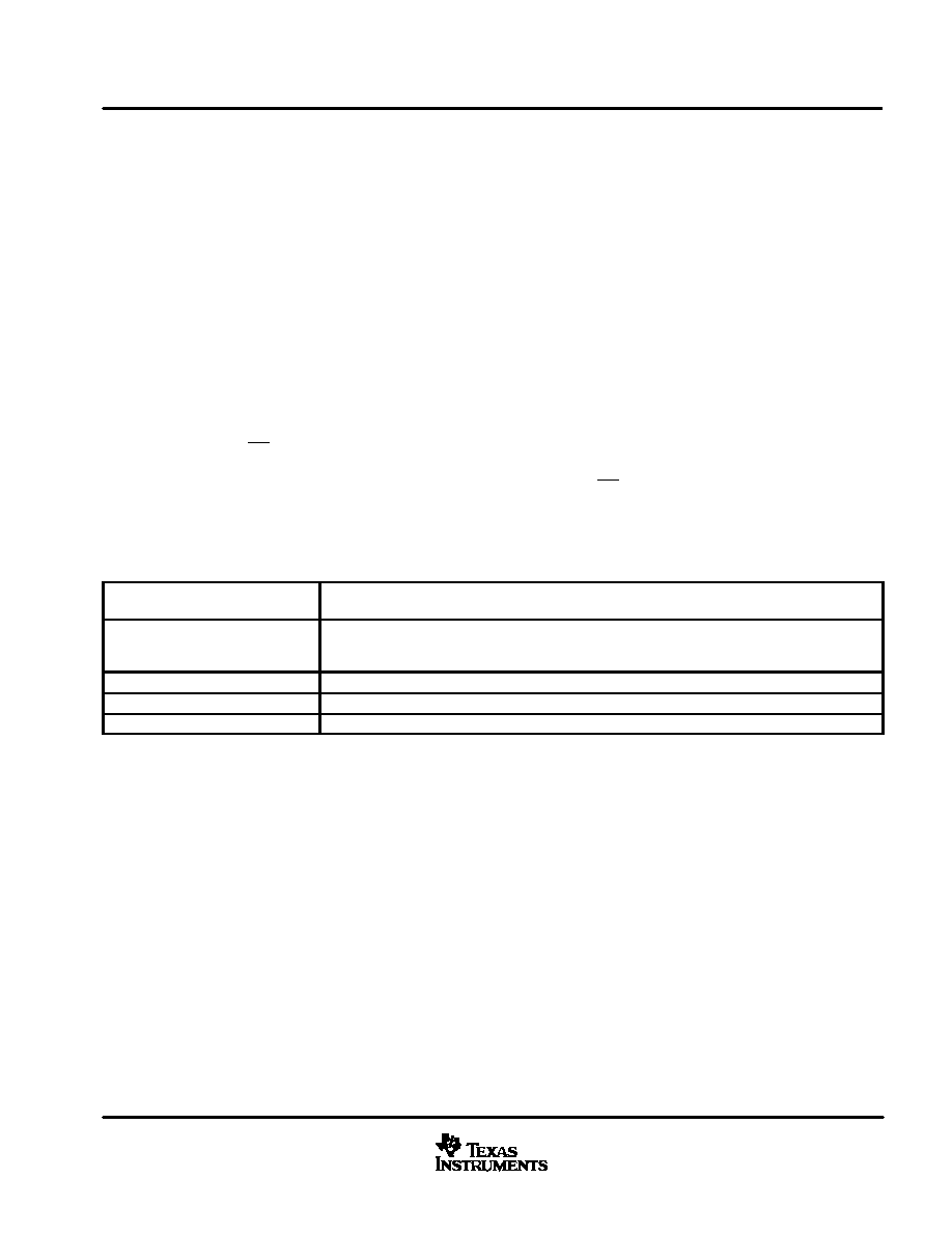
Table 1. Operational Terminology
Current (N) I/O cycle
The entire I/O CLOCK sequence that transfers address and control data into the data register and clocks
the digital result from the previous conversion from DATA OUT
Current (N) conversion cycle
The conversion cycle starts immediately after the current I/O cycle. The end of the current I/O cycle is the
last clock falling edge in the I/O CLOCK sequence. The current conversion result is loaded into the out-
put register when conversion is complete.
Current (N) conversion result
The current conversion result is serially shifted out on the next I/O cycle.
Previous (N–1) conversion cycle
The conversion cycle just prior to the current I/O cycle
Next (N+1) I/O cycle
The I/O period that follows the current conversion cycle
Example:
In 12-bit mode, the result of the current conversion cycle is a 12-bit serial-data stream clocked out during the
next I/O cycle. The current I/O cycle must be exactly 12 bits long to maintain synchronization, even when this
corrupts the output data from the previous conversion. The current conversion is begun immediately after the
twelfth falling edge of the current I/O cycle.
data input
The data input is internally connected to an 8-bit serial-input address and control register. The register defines
the operation of the converter and the output data length. The host provides the input data byte with the MSB
first. Each data bit is clocked in on the rising edge of the I/O CLOCK sequence (see Table 2 for the data
input-register format).
相關(guān)PDF資料 |
PDF描述 |
|---|---|
| TLV2553IPWG4 | 11-CH 12-BIT SUCCESSIVE APPROXIMATION ADC, SERIAL ACCESS, PDSO20 |
| TLV2553IPW | 11-CH 12-BIT SUCCESSIVE APPROXIMATION ADC, SERIAL ACCESS, PDSO20 |
| TLV2553IDWR | 11-CH 12-BIT SUCCESSIVE APPROXIMATION ADC, SERIAL ACCESS, PDSO20 |
| TLV2553IDWRQ1 | 11-CH 12-BIT SUCCESSIVE APPROXIMATION ADC, SERIAL ACCESS, PDSO20 |
| TLV2556IDWRG4 | 11-CH 12-BIT SUCCESSIVE APPROXIMATION ADC, SERIAL ACCESS, PDSO20 |
相關(guān)代理商/技術(shù)參數(shù) |
參數(shù)描述 |
|---|---|
| TLV2553IDWG4 | 功能描述:模數(shù)轉(zhuǎn)換器 - ADC 12-Bit 200 KSPS 11 Ch Lo-Pwr RoHS:否 制造商:Texas Instruments 通道數(shù)量:2 結(jié)構(gòu):Sigma-Delta 轉(zhuǎn)換速率:125 SPs to 8 KSPs 分辨率:24 bit 輸入類型:Differential 信噪比:107 dB 接口類型:SPI 工作電源電壓:1.7 V to 3.6 V, 2.7 V to 5.25 V 最大工作溫度:+ 85 C 安裝風格:SMD/SMT 封裝 / 箱體:VQFN-32 |
| TLV2553IDWR | 功能描述:模數(shù)轉(zhuǎn)換器 - ADC 12bit 200kSPS ADC RoHS:否 制造商:Texas Instruments 通道數(shù)量:2 結(jié)構(gòu):Sigma-Delta 轉(zhuǎn)換速率:125 SPs to 8 KSPs 分辨率:24 bit 輸入類型:Differential 信噪比:107 dB 接口類型:SPI 工作電源電壓:1.7 V to 3.6 V, 2.7 V to 5.25 V 最大工作溫度:+ 85 C 安裝風格:SMD/SMT 封裝 / 箱體:VQFN-32 |
| TLV2553IDWRG4 | 功能描述:模數(shù)轉(zhuǎn)換器 - ADC 12-Bit 200 KSPS 11 Ch Lo-Pwr RoHS:否 制造商:Texas Instruments 通道數(shù)量:2 結(jié)構(gòu):Sigma-Delta 轉(zhuǎn)換速率:125 SPs to 8 KSPs 分辨率:24 bit 輸入類型:Differential 信噪比:107 dB 接口類型:SPI 工作電源電壓:1.7 V to 3.6 V, 2.7 V to 5.25 V 最大工作溫度:+ 85 C 安裝風格:SMD/SMT 封裝 / 箱體:VQFN-32 |
| TLV2553IDWRQ1 | 功能描述:模數(shù)轉(zhuǎn)換器 - ADC Auto Cat 12B 200KSPS 11Ch Low-Pwr Ser ADC RoHS:否 制造商:Texas Instruments 通道數(shù)量:2 結(jié)構(gòu):Sigma-Delta 轉(zhuǎn)換速率:125 SPs to 8 KSPs 分辨率:24 bit 輸入類型:Differential 信噪比:107 dB 接口類型:SPI 工作電源電壓:1.7 V to 3.6 V, 2.7 V to 5.25 V 最大工作溫度:+ 85 C 安裝風格:SMD/SMT 封裝 / 箱體:VQFN-32 |
| TLV2553IPW | 功能描述:模數(shù)轉(zhuǎn)換器 - ADC 12-Bit 200 KSPS 11 Ch Lo-Pwr RoHS:否 制造商:Texas Instruments 通道數(shù)量:2 結(jié)構(gòu):Sigma-Delta 轉(zhuǎn)換速率:125 SPs to 8 KSPs 分辨率:24 bit 輸入類型:Differential 信噪比:107 dB 接口類型:SPI 工作電源電壓:1.7 V to 3.6 V, 2.7 V to 5.25 V 最大工作溫度:+ 85 C 安裝風格:SMD/SMT 封裝 / 箱體:VQFN-32 |
發(fā)布緊急采購,3分鐘左右您將得到回復。