- 您現(xiàn)在的位置:買賣IC網(wǎng) > PDF目錄98253 > TLV320AIC20KIPFBRG4 (TEXAS INSTRUMENTS INC) SPECIALTY CONSUMER CIRCUIT, PQFP48 PDF資料下載
參數(shù)資料
| 型號(hào): | TLV320AIC20KIPFBRG4 |
| 廠商: | TEXAS INSTRUMENTS INC |
| 元件分類: | 消費(fèi)家電 |
| 英文描述: | SPECIALTY CONSUMER CIRCUIT, PQFP48 |
| 封裝: | GREEN, PLASTIC, TQFP-48 |
| 文件頁數(shù): | 31/52頁 |
| 文件大小: | 981K |
| 代理商: | TLV320AIC20KIPFBRG4 |
第1頁第2頁第3頁第4頁第5頁第6頁第7頁第8頁第9頁第10頁第11頁第12頁第13頁第14頁第15頁第16頁第17頁第18頁第19頁第20頁第21頁第22頁第23頁第24頁第25頁第26頁第27頁第28頁第29頁第30頁當(dāng)前第31頁第32頁第33頁第34頁第35頁第36頁第37頁第38頁第39頁第40頁第41頁第42頁第43頁第44頁第45頁第46頁第47頁第48頁第49頁第50頁第51頁第52頁

www.ti.com
S/Sr
I2C Device Address (3 Bit)+
SMARTDM Device Address +
R/W
= 0
Mode (5 Bit) + Index
Register Address
(3 Bit)
Ack
Control Register
Data (Write)
Ack
Control Register
Data (Write)
7 Bit
1 Bit
8 Bit
Increment Index Register Address
Default/Broadcast
(00000/11111)
Write Mode
To the Address Given
by Index Register
Address
To the Address Given
by Index Register
Address
S/Sr I2C Device Address (3 Bit)+
SMARTDM Device Address +
R/W
= 1
Control Register Data
(Read)
Ack
Control Register
Data (Read)
Ack
7 Bit
1 Bit
8 Bit
Read Mode
From the Address Given
by Index Register Address
From the Address Given
by Index Register Address
Increment Index
Register Address
Increment Index
Register Address
S/Sr I2C Device Address (3 Bit)+
SMARTDM Device Address +
R/W
= 0
Mode (5 Bit) + Index
Register Address
(3 Bit)
Ack
7 Bit
1 Bit
8 Bit
For Initializing Index Register Address
Stop
Register Map
TLV320AIC20, TLV320AIC21
TLV320AIC24, TLV320AIC25
TLV320AIC20K, TLV320AIC24K
SLAS363D – MARCH 2002 – REVISED APRIL 2005
S/Sr -> Start/Repeated Start.
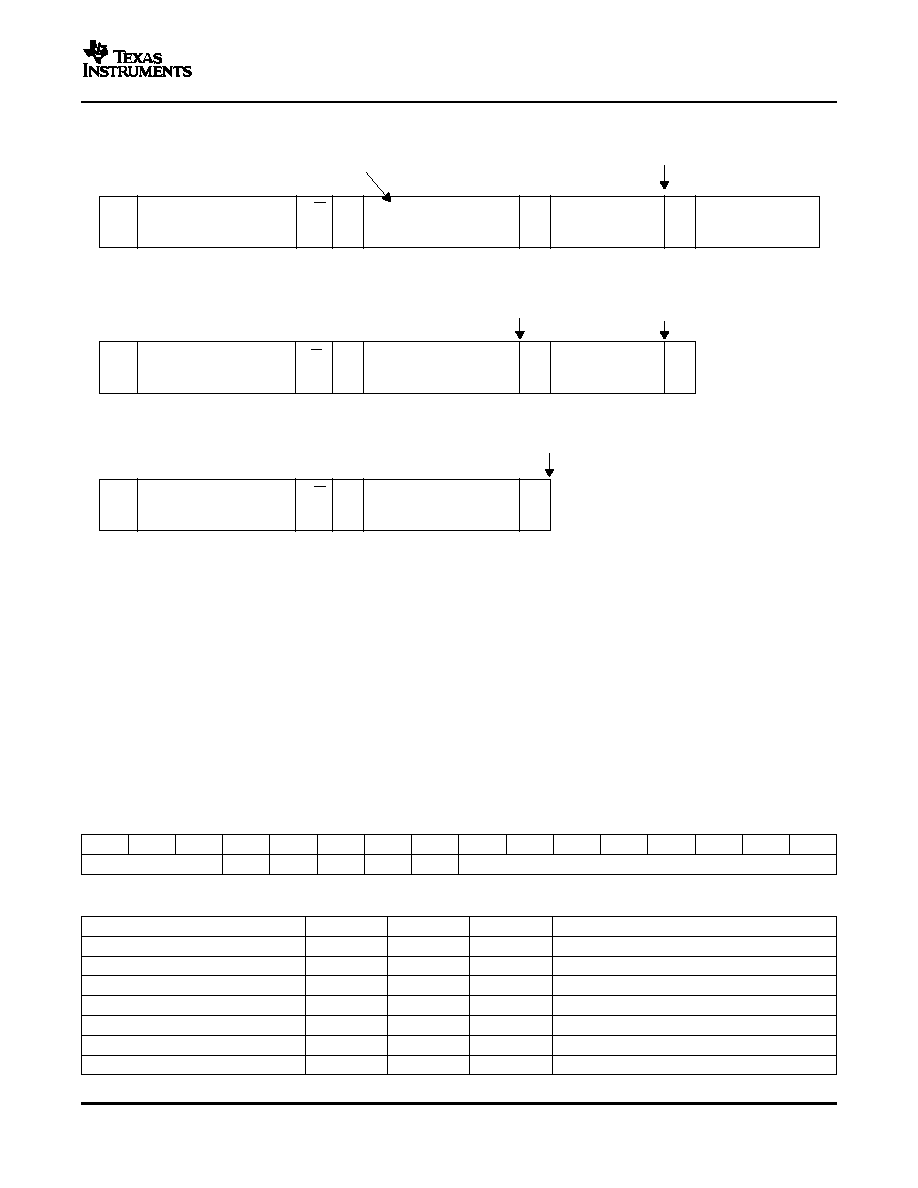
Figure 33. Index Register Addresses
Each AIC2x codec consists of 2 channels. Each channel has 6 registers to enable the user to control various
components. Registers that control resources that are common across the two channels are shadowed. This
means that writing to the appropriate register in one channel automatically updates the contents of the same
register in the other channel to reflect the change. For example, writing to register 4 in channel 1 automatically
updates the contents of register 4 for channel 2 and vice versa. Refer to the individual register description for a
more detailed description of the exact register bits that are shadowed. Bits D15 through D13 represent the
control register address that is written with data carried in D7 through D0. Bit D12 determines a read or a write
cycle to the addressed register. When D12 = 0, a write cycle is selected. When D12 = 1, a read cycle is selected.
Bit D11 controls the broadcast mode as described above, in which the broadcast mode is enabled if D11 is set to
1. Always write 1s to the bits D10 through D8.
Table 3 shows the register map.
Table 3. Register Map
D15
D14
D13
D12
D11
D10
D9
D8
D7
D6
D5
D4
D3
D2
D1
D0
Register Address
RW
BC
1
Control Register Content
Table 4. Register Addressing
REGISTER NO.
D15
D14
D13
REGISTER NAME
0
No operation
1
0
1
Control 1
2
0
1
0
Control 2
3
0
1
Control 3
4
1
0
Control 4
5
1
0
1
Control 5
6
1
0
Control 6
37
相關(guān)PDF資料 |
PDF描述 |
|---|---|
| TLV320AIC26IRHBR | SPECIALTY CONSUMER CIRCUIT, PQCC32 |
| TLV320AIC26IRHB | SPECIALTY CONSUMER CIRCUIT, PQCC32 |
| TLV320AIC26IRHBG4 | SPECIALTY CONSUMER CIRCUIT, PQCC32 |
| TLV320AIC26IRHBRG4 | SPECIALTY CONSUMER CIRCUIT, PQCC32 |
| TLV320AIC27CPFB | SPECIALTY CONSUMER CIRCUIT, PQFP48 |
相關(guān)代理商/技術(shù)參數(shù) |
參數(shù)描述 |
|---|---|
| TLV320AIC21 | 制造商:TI 制造商全稱:Texas Instruments 功能描述:Layout and Grounding Guidelines for TLV320AIC2x |
| TLV320AIC21C | 制造商:TI 制造商全稱:Texas Instruments 功能描述:Layout and Grounding Guidelines for TLV320AIC2x |
| TLV320AIC21CPFB | 功能描述:接口—CODEC Low Power Low IOVdd Dual Channel RoHS:否 制造商:Texas Instruments 類型: 分辨率: 轉(zhuǎn)換速率:48 kSPs 接口類型:I2C ADC 數(shù)量:2 DAC 數(shù)量:4 工作電源電壓:1.8 V, 2.1 V, 2.3 V to 5.5 V 最大工作溫度:+ 85 C 安裝風(fēng)格:SMD/SMT 封裝 / 箱體:DSBGA-81 封裝:Reel |
| TLV320AIC21CPFBG4 | 功能描述:接口—CODEC 64 x 18 3.3-V Synch FIFO Memory RoHS:否 制造商:Texas Instruments 類型: 分辨率: 轉(zhuǎn)換速率:48 kSPs 接口類型:I2C ADC 數(shù)量:2 DAC 數(shù)量:4 工作電源電壓:1.8 V, 2.1 V, 2.3 V to 5.5 V 最大工作溫度:+ 85 C 安裝風(fēng)格:SMD/SMT 封裝 / 箱體:DSBGA-81 封裝:Reel |
| TLV320AIC21CPFBR | 功能描述:接口—CODEC Low Power Low IOVdd Dual Channel RoHS:否 制造商:Texas Instruments 類型: 分辨率: 轉(zhuǎn)換速率:48 kSPs 接口類型:I2C ADC 數(shù)量:2 DAC 數(shù)量:4 工作電源電壓:1.8 V, 2.1 V, 2.3 V to 5.5 V 最大工作溫度:+ 85 C 安裝風(fēng)格:SMD/SMT 封裝 / 箱體:DSBGA-81 封裝:Reel |
發(fā)布緊急采購(gòu),3分鐘左右您將得到回復(fù)。