- 您現(xiàn)在的位置:買賣IC網(wǎng) > PDF目錄98262 > TLV5637IDR (TEXAS INSTRUMENTS INC) SERIAL INPUT LOADING, 2.8 us SETTLING TIME, 10-BIT DAC, PDSO8 PDF資料下載
參數(shù)資料
| 型號(hào): | TLV5637IDR |
| 廠商: | TEXAS INSTRUMENTS INC |
| 元件分類: | DAC |
| 英文描述: | SERIAL INPUT LOADING, 2.8 us SETTLING TIME, 10-BIT DAC, PDSO8 |
| 封裝: | GREEN, PLASTIC, MS-012AA, SOIC-8 |
| 文件頁(yè)數(shù): | 2/21頁(yè) |
| 文件大?。?/td> | 422K |
| 代理商: | TLV5637IDR |
第1頁(yè)當(dāng)前第2頁(yè)第3頁(yè)第4頁(yè)第5頁(yè)第6頁(yè)第7頁(yè)第8頁(yè)第9頁(yè)第10頁(yè)第11頁(yè)第12頁(yè)第13頁(yè)第14頁(yè)第15頁(yè)第16頁(yè)第17頁(yè)第18頁(yè)第19頁(yè)第20頁(yè)第21頁(yè)

www.ti.com
APPLICATION INFORMATION
GENERAL FUNCTION
2 REF
CODE
0x1000
[V]
SERIAL INTERFACE
TMS320
DSP FSX
CLKX
DX
TLV5637
SCLK
DIN
CS
SPI
I/O
SCK
MOSI
TLV5637
SCLK
DIN
CS
Microwire
I/O
SK
SO
TLV5637
SCLK
DIN
CS
SERIAL CLOCK FREQUENCY AND UPDATE RATE
f
sclkmax =
1
(t
+t
)
whmin
wlmin
=20MHz
f
=
updatemax
1
16(t
+t
)
whmin
wlmin
=1.25MHz
SLAS224C – JUNE 1999 – REVISED JUNE 2007
The TLV5637 is a dual 10-bit, single supply DAC, based on a resistor string architecture. It consists of a serial
interface, a speed and power-down control logic, a programmable internal reference, a resistor string, and a
rail-to-rail output buffer.
The output voltage (full scale determined by reference) is given by:
Where REF is the reference voltage and CODE is the digital input value in the range 0x000 to 0xFFF. Because
it is a 10-bit DAC, only D11 to D2 are used. D0 and D1 are ignored. A power-on reset initially puts the internal
latches to a defined state (all bits zero).
A falling edge of CS starts shifting the data bit-per-bit (starting with the MSB) to the internal register on the falling
edges of SCLK. After 16 bits have been transferred or CS rises, the content of the shift register is moved to the
target latches (DAC A, DAC B, BUFFER, CONTROL), depending on the control bits within the data word.
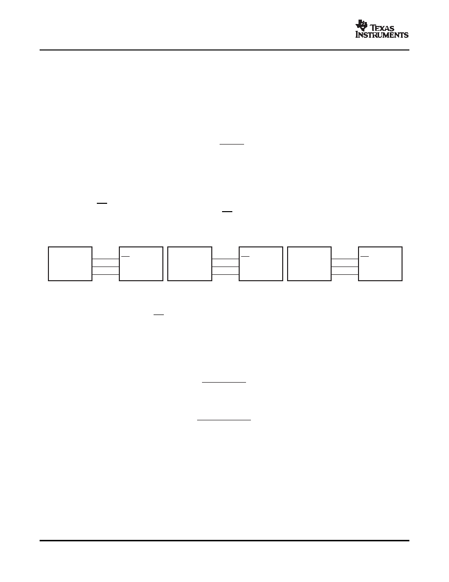
Figure 13 shows examples of how to connect the TLV5637 to TMS320, SPI, and Microwire.
Figure 13. Three-Wire Interface
Notes on SPI and Microwire: Before the controller starts the data transfer, the software has to generate a falling
edge on the I/O pin connected to CS. If the word width is 8 bits (SPI and Microwire), two write operations must
be performed to program the TLV5637. After the write operation(s), the holding registers or the control register
are updated automatically on the 16th positive clock edge.
The maximum serial clock frequency is given by:
The maximum update rate is:
Note that the maximum update rate is just a theoretical value for the serial interface, as the settling time of the
TLV5637 has to be considered as well.
10
相關(guān)PDF資料 |
PDF描述 |
|---|---|
| TLV5637CD | SERIAL INPUT LOADING, 2.8 us SETTLING TIME, 10-BIT DAC, PDSO8 |
| TLV5637IDG4 | SERIAL INPUT LOADING, 2.8 us SETTLING TIME, 10-BIT DAC, PDSO8 |
| TLV5638QDREP | SERIAL INPUT LOADING, 3.5 us SETTLING TIME, 12-BIT DAC, PDSO8 |
| TLV5638MDREP | SERIAL INPUT LOADING, 3.5 us SETTLING TIME, 12-BIT DAC, PDSO8 |
| TLV5639CDWRG4 | PARALLEL, WORD INPUT LOADING, 3.5 us SETTLING TIME, 12-BIT DAC, PDSO20 |
相關(guān)代理商/技術(shù)參數(shù) |
參數(shù)描述 |
|---|---|
| TLV5637IDRG4 | 功能描述:數(shù)模轉(zhuǎn)換器- DAC 10Bit/1us DAC Serial Input Dual DAC RoHS:否 制造商:Texas Instruments 轉(zhuǎn)換器數(shù)量:1 DAC 輸出端數(shù)量:1 轉(zhuǎn)換速率:2 MSPs 分辨率:16 bit 接口類型:QSPI, SPI, Serial (3-Wire, Microwire) 穩(wěn)定時(shí)間:1 us 最大工作溫度:+ 85 C 安裝風(fēng)格:SMD/SMT 封裝 / 箱體:SOIC-14 封裝:Tube |
| TLV5638 | 制造商:TI 制造商全稱:Texas Instruments 功能描述:2.7 V TO 5.5 V LOW POWER DUAL 12-BIT DIGITAL-TO-ANALOG CONVERTER WITH INTERNAL REFERENCE AND POWER DOWN |
| TLV5638_12 | 制造商:TI 制造商全稱:Texas Instruments 功能描述:2.7-V TO 5.5-V LOW-POWER DUAL 12-BIT DIGITAL-TO-ANALOG CONVERTER WITH INTERNAL REFERENCE AND POWER DOWN |
| TLV5638CD | 功能描述:數(shù)模轉(zhuǎn)換器- DAC Dual 12bit Low Power RoHS:否 制造商:Texas Instruments 轉(zhuǎn)換器數(shù)量:1 DAC 輸出端數(shù)量:1 轉(zhuǎn)換速率:2 MSPs 分辨率:16 bit 接口類型:QSPI, SPI, Serial (3-Wire, Microwire) 穩(wěn)定時(shí)間:1 us 最大工作溫度:+ 85 C 安裝風(fēng)格:SMD/SMT 封裝 / 箱體:SOIC-14 封裝:Tube |
| TLV5638CDG4 | 功能描述:數(shù)模轉(zhuǎn)換器- DAC 2.7-5.5-V Low Power Dual 12-Bit DAC RoHS:否 制造商:Texas Instruments 轉(zhuǎn)換器數(shù)量:1 DAC 輸出端數(shù)量:1 轉(zhuǎn)換速率:2 MSPs 分辨率:16 bit 接口類型:QSPI, SPI, Serial (3-Wire, Microwire) 穩(wěn)定時(shí)間:1 us 最大工作溫度:+ 85 C 安裝風(fēng)格:SMD/SMT 封裝 / 箱體:SOIC-14 封裝:Tube |
發(fā)布緊急采購(gòu),3分鐘左右您將得到回復(fù)。