- 您現(xiàn)在的位置:買賣IC網(wǎng) > PDF目錄368677 > TMS370C768AFNT 8-BIT MICROCONTROLLER PDF資料下載
參數(shù)資料
| 型號: | TMS370C768AFNT |
| 元件分類: | 8位微控制器 |
| 英文描述: | 8-BIT MICROCONTROLLER |
| 中文描述: | 8位微控制器 |
| 文件頁數(shù): | 45/48頁 |
| 文件大小: | 711K |
| 代理商: | TMS370C768AFNT |
第1頁第2頁第3頁第4頁第5頁第6頁第7頁第8頁第9頁第10頁第11頁第12頁第13頁第14頁第15頁第16頁第17頁第18頁第19頁第20頁第21頁第22頁第23頁第24頁第25頁第26頁第27頁第28頁第29頁第30頁第31頁第32頁第33頁第34頁第35頁第36頁第37頁第38頁第39頁第40頁第41頁第42頁第43頁第44頁當(dāng)前第45頁第46頁第47頁第48頁
TMS370Cx36
8-BIT MICROCONTROLLER
SPNS039B – JANUARY 1996 – REVISED FEBRUARY 1997
45
POST OFFICE BOX 1443
HOUSTON, TEXAS 77251–1443
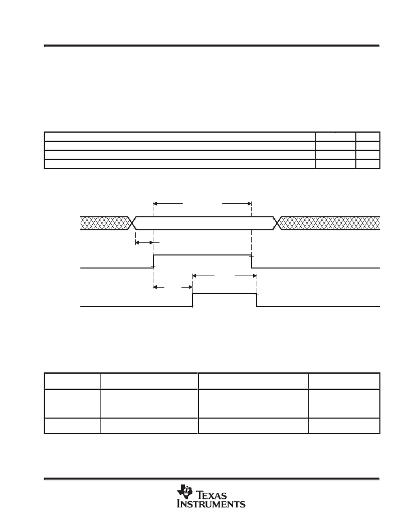
ADC1 converter (continued)
The ADC1 module allows complete freedom in design of the sources for the analog inputs. The period of the
sample time is user-defined so that the high-impedance can be accommodated without penalty to the
low-impedance sources. The sample period begins when the SAMPLE START bit of the ADC1 control register
(ADCTL.6) is set to 1. The end of the signal sample period occurs when the conversion bit (CONVERT START,
ADCTL.7) is set to 1. After a hold time, the converter will reset the SAMPLE START and CONVERT START bits,
signaling that a conversion has started and that the analog signal can be removed.
analog timing requirements (see Figure 22)
MIN
MAX
UNIT
tsu(S)
th(AN)
tw(S)
The value given is valid for a signal with a source impedance > 1 k
. If the source impedance is < 1 k
, use a minimum sampling time of 1
μ
s.
Setup time, analog to sample command
0
ns
Hold time, analog input from start of conversion
Pulse duration, sample time per kilo-
of source impedance
18tc
ns
1
μ
s/k
Analog In
Sample Start
Convert Start
Analog Stable
th(AN)
tw(S)
tsu(S)
Figure 22. Analog Timing
Table 19 is designed to aid the user in referencing a device part number to a mechanical drawing. The table
shows a cross-reference of the device part number to the TMS370 generic package name and the associated
mechanical drawing by drawing number and name.
Table 19. TMS370Cx36 Family Package Type and Mechanical Cross-Reference
áááááááááááááááááááááááááááááá
áááááááááááááááááááááááááááááá
á
á
áááááááááááááááááááááááááááááá
á
áááááááááááááááááááááááááááááá
(mil pin spacing)
á
á
MECHANICAL NAME
á
áááá
(50-mil pin spacing)
áááá
á
(CLCC)
ááááááááá
(PLCC)
á
PLASTIC LEADED CHIP CARRIER
ááááááááá
ááááááááá
á
áááááá
áááááá
áááááá
TMS370C036AFNT
á
á
TMS370C036AFNA
á
á
CERAMIC LEADED CHIP CARRIER
á
á
SE370C736AFZT
相關(guān)PDF資料 |
PDF描述 |
|---|---|
| TMS370C768AYYZ | Microcontroller |
| TMS370C769AFNT | 8-BIT MICROCONTROLLER |
| TMS370C769AYYZ | Microcontroller |
| TMS370C777AFNT | 8-BIT MICROCONTROLLER |
| TMS370C777ANMT | 8-BIT MICROCONTROLLER |
相關(guān)代理商/技術(shù)參數(shù) |
參數(shù)描述 |
|---|---|
| TMS370C769AFNT | 制造商:Rochester Electronics LLC 功能描述:8BIT TMS370 CISC 48KB OTP 5MHZ 5V 68PLCC - Tape and Reel 制造商:Texas Instruments 功能描述: |
| TMS370C777AFNT | 制造商:Rochester Electronics LLC 功能描述:8BIT TMS370 CISC 24KB OTP 5MHZ 5V 68PLCC - Bulk 制造商:Texas Instruments 功能描述: |
| TMS370C777ANMT | 制造商:Rochester Electronics LLC 功能描述:8BIT TMS370 CISC 24KB OTP 5MHZ 5V 64SDIP - Tape and Reel 制造商:Texas Instruments 功能描述: |
| TMS370C792FNT | 制造商:Rochester Electronics LLC 功能描述:- Tape and Reel |
| TMS370C792N2T | 制造商:Rochester Electronics LLC 功能描述:- Bulk |
發(fā)布緊急采購,3分鐘左右您將得到回復(fù)。