- 您現(xiàn)在的位置:買賣IC網(wǎng) > PDF目錄382646 > TMX320C6204GFN167 (Texas Instruments, Inc.) FIXED-POINT DIGITAL SIGNAL PROCESSORS PDF資料下載
參數(shù)資料
| 型號(hào): | TMX320C6204GFN167 |
| 廠商: | Texas Instruments, Inc. |
| 元件分類: | 數(shù)字信號(hào)處理 |
| 英文描述: | FIXED-POINT DIGITAL SIGNAL PROCESSORS |
| 中文描述: | 定點(diǎn)數(shù)字信號(hào)處理器 |
| 文件頁(yè)數(shù): | 33/83頁(yè) |
| 文件大小: | 1176K |
| 代理商: | TMX320C6204GFN167 |
第1頁(yè)第2頁(yè)第3頁(yè)第4頁(yè)第5頁(yè)第6頁(yè)第7頁(yè)第8頁(yè)第9頁(yè)第10頁(yè)第11頁(yè)第12頁(yè)第13頁(yè)第14頁(yè)第15頁(yè)第16頁(yè)第17頁(yè)第18頁(yè)第19頁(yè)第20頁(yè)第21頁(yè)第22頁(yè)第23頁(yè)第24頁(yè)第25頁(yè)第26頁(yè)第27頁(yè)第28頁(yè)第29頁(yè)第30頁(yè)第31頁(yè)第32頁(yè)當(dāng)前第33頁(yè)第34頁(yè)第35頁(yè)第36頁(yè)第37頁(yè)第38頁(yè)第39頁(yè)第40頁(yè)第41頁(yè)第42頁(yè)第43頁(yè)第44頁(yè)第45頁(yè)第46頁(yè)第47頁(yè)第48頁(yè)第49頁(yè)第50頁(yè)第51頁(yè)第52頁(yè)第53頁(yè)第54頁(yè)第55頁(yè)第56頁(yè)第57頁(yè)第58頁(yè)第59頁(yè)第60頁(yè)第61頁(yè)第62頁(yè)第63頁(yè)第64頁(yè)第65頁(yè)第66頁(yè)第67頁(yè)第68頁(yè)第69頁(yè)第70頁(yè)第71頁(yè)第72頁(yè)第73頁(yè)第74頁(yè)第75頁(yè)第76頁(yè)第77頁(yè)第78頁(yè)第79頁(yè)第80頁(yè)第81頁(yè)第82頁(yè)第83頁(yè)
TMS320C6211, TMS320C6211B
FIXED-POINT DIGITAL SIGNAL PROCESSORS
SPRS073K
AUGUST 1998
REVISED MARCH 2004
33
POST OFFICE BOX 1443
HOUSTON, TEXAS 77251
1443
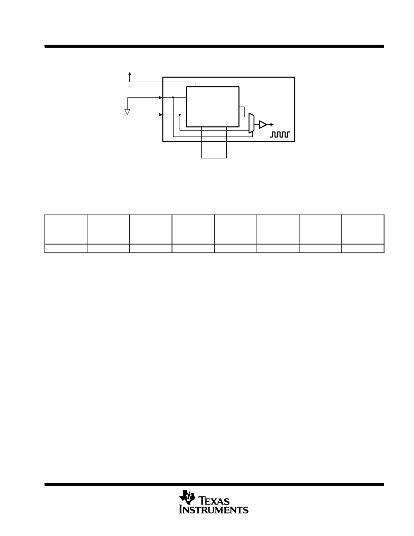
clock PLL (continued)
CLKMODE0
PLL
PLLV
CLKIN
LOOP FILTER
PLLCLK
PLLMULT
CLKIN
P
Internal to
C6211/C6211B
CPU
CLOCK
P
1
0
3.3V
NOTES: A. For a system with ONLY PLL x1 (bypass) mode, short the PLLF terminal to the PLLG terminal.
B. The 3.3-V supply for the EMI filter must be from the same 3.3-V power plane supplying the I/O voltage, DV
DD
.
Figure 6. External PLL Circuitry for x1 (Bypass) Mode Only
Table 19. C6211/C6211B PLL Component Selection
CLKMODE
CLKIN
RANGE
(MHz)
CPU CLOCK
FREQUENCY
(CLKOUT1)
RANGE (MHz)
65
167
CLKOUT2
RANGE
(MHz)
R1 [
±
1%]
(
)
C1 [
±
10%]
(nF)
C2 [
±
10%]
(pF)
TYPICAL
LOCK TIME
(
μ
s)
x4
16.3
41.6
32.5
83
60.4
27
560
75
Under some operating conditions, the maximum PLL lock time may vary as much as 150% from the specified typical value. For example, if the
typical lock time is specified as 100
μ
s, the maximum value may be as long as 250
μ
s.
發(fā)布緊急采購(gòu),3分鐘左右您將得到回復(fù)。