- 您現(xiàn)在的位置:買賣IC網(wǎng) > PDF目錄382662 > TOP242F SMPS Controller PDF資料下載
參數(shù)資料
| 型號: | TOP242F |
| 英文描述: | SMPS Controller |
| 中文描述: | 開關(guān)電源控制器 |
| 文件頁數(shù): | 5/52頁 |
| 文件大小: | 457K |
| 代理商: | TOP242F |
第1頁第2頁第3頁第4頁當(dāng)前第5頁第6頁第7頁第8頁第9頁第10頁第11頁第12頁第13頁第14頁第15頁第16頁第17頁第18頁第19頁第20頁第21頁第22頁第23頁第24頁第25頁第26頁第27頁第28頁第29頁第30頁第31頁第32頁第33頁第34頁第35頁第36頁第37頁第38頁第39頁第40頁第41頁第42頁第43頁第44頁第45頁第46頁第47頁第48頁第49頁第50頁第51頁第52頁

TOP242-250
5
H
9/02
TOPSwitch-GX
Family Functional Description
Like
TOPSwitch
,
TOPSwitch-GX
is an integrated switched
mode power supply chip that converts a current at the control
input to a duty cycle at the open drain output of a high voltage
power MOSFET. During normal operation the duty cycle of
the power MOSFET decreases linearly with increasing
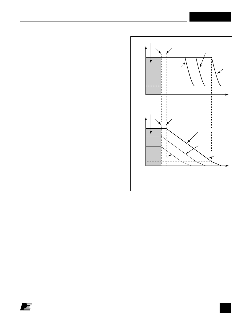
CONTROL pin current as shown in Figure 7.
In addition to the three terminal
TOPSwitch
features, such as
the high voltage start-up, the cycle-by-cycle current limiting,
loop compensation circuitry, auto-restart, thermal shutdown,
the
TOPSwitch-GX
incorporates many additional functions that
reduce system cost, increase power supply performance and
design flexibility. A patented high voltage CMOS technology
allows both the high voltage power MOSFET and all the low
voltage control circuitry to be cost effectively integrated onto
a single monolithic chip.
Three terminals, FREQUENCY, LINE-SENSE, and EXTER-
NAL CURRENT LIMIT (available in Y, R or F package) or
one terminal MULTI-FUNCTION (available in P or G
Package) have been added to implement some of the new
functions. These terminals can be connected to the SOURCE
pin to operate the
TOPSwitch-GX
in a
TOPSwitch
-like three
terminal mode. However, even in this three terminal mode, the
TOPSwitch-GX
offers many new transparent features that do
not require any external components:
1. A fully integrated 10 ms soft-start limits peak currents and
voltages during start-up and dramatically reduces or
eliminates output overshoot in most applications.
2. DC
of 78% allows smaller input storage capacitor, lower
input voltage requirement and/or higher power capability.
3. Frequency reduction at light loads lowers the switching
losses and maintains good cross regulation in multiple
output supplies.
4. Higher switching frequency of 132 kHz reduces the
transformer size with no noticeable impact on EMI.
5. Frequency jittering reduces EMI.
6. Hysteretic over-temperature shutdown ensures automatic
recovery from thermal fault. Large hysteresis prevents circuit
board overheating.
7. Packages with omitted pins and lead forming provide large
drain creepage distance.
8. Tighter absolute tolerances and smaller temperature vari-
ations on switching frequency, current limit and PWM gain.
The LINE-SENSE (L) pin is usually used for line sensing by
connecting a resistor from this pin to the rectified DC high
voltage bus to implement line overvoltage (OV), under-voltage
(UV) and line feed forward with DC
reduction. In this
mode, the value of the resistor determines the OV/UV thresholds
and the DC
is reduced linearly starting from a line voltage
above the under-voltage threshold. See Table 2 and Figure 11.
The pin can also be used as a remote ON/OFF and a
synchronization input.
The EXTERNAL CURRENT LIMIT (X) pin is usually used to
reduce the current limit externally to a value close to the operat-
ing peak current, by connecting the pin to SOURCE through a
resistor. This pin can also be used as a remote ON/OFF and a
synchronization input in both modes. See Table 2 and Figure 11.
For the P or G packages the LINE-SENSE and EXTERNAL
CURRENT LIMIT pin functions are combined on one MULTI-
FUNCTION (M) pin. However, some of the functions become
mutually exclusive as shown in Table 3.
The FREQUENCY (F) pin in the Y, R or F package sets the
switching frequency to the default value of 132 kHz when
connected to SOURCE pin. A half frequency option of 66 kHz
can be chosen by connecting this pin to CONTROL pin
instead. Leaving this pin open is not recommended.
PI-2633-011502
D
I
C
(mA)
TOP242-5 1.6 2.0
TOP246-9 2.2 2.6
TOP250 2.4 2.7
5.2 6.0
5.8 6.6
6.5 7.3
I
CD1
I
B
Auto-restart
I
L
= 125
μ
A
I
L
< I
L(DC)
I
L
= 190
μ
A
78
10
38
F
I
C
(mA)
30
I
CD1
I
B
Auto-restart
132
Note: For P and G packages I
L
is replaced with I
M
.
I
L
< I
L(DC)
I
L
= 125
μ
A
Slope = PWM Gain
I
L
= 190
μ
A
Figure 7. Relationship of Duty Cycle and Frequency to CONTROL
Pin Current.
相關(guān)PDF資料 |
PDF描述 |
|---|---|
| TOP242G-TL | SMPS Controller |
| TOP242R-TL | SMPS Controller |
| TOP243F | SMPS Controller |
| TOP243G | SMPS Controller |
| TOP243G-TL | SMPS Controller |
相關(guān)代理商/技術(shù)參數(shù) |
參數(shù)描述 |
|---|---|
| TOP242F- | 制造商:POWERINT 制造商全稱:Power Integrations, Inc. 功能描述:TOPSwitch-GX Family Extended Power, Design Flexible, EcoSmart, Integrated Off-line Switcher |
| TOP242FN | 功能描述:交流/直流開關(guān)轉(zhuǎn)換器 10W 85-265 VAC 15 W230 VAC RoHS:否 制造商:STMicroelectronics 輸出電壓:800 V 輸入/電源電壓(最大值):23.5 V 輸入/電源電壓(最小值):11.5 V 開關(guān)頻率:115 kHz 電源電流:1.6 mA 工作溫度范圍:- 40 C to + 150 C 安裝風(fēng)格:SMD/SMT 封裝 / 箱體:SSO-10 封裝:Reel |
| TOP242FN- | 制造商:POWERINT 制造商全稱:Power Integrations, Inc. 功能描述:TOPSwitch-GX Family Extended Power, Design Flexible, EcoSmart, Integrated Off-line Switcher |
| TOP242FN-TL | 制造商:POWERINT 制造商全稱:Power Integrations, Inc. 功能描述:TOPSwitch-GX Family Extended Power, Design Flexible, EcoSmart, Integrated Off-line Switcher |
| TOP242F-TL | 制造商:POWERINT 制造商全稱:Power Integrations, Inc. 功能描述:TOPSwitch-GX Family Extended Power, Design Flexible, EcoSmart, Integrated Off-line Switcher |
發(fā)布緊急采購,3分鐘左右您將得到回復(fù)。