- 您現(xiàn)在的位置:買賣IC網(wǎng) > PDF目錄373680 > TORX141P (Toshiba Corporation) FIBER OPTIC RECEIVING MODULE PDF資料下載
參數(shù)資料
| 型號: | TORX141P |
| 廠商: | Toshiba Corporation |
| 英文描述: | FIBER OPTIC RECEIVING MODULE |
| 中文描述: | 光纖接收模塊 |
| 文件頁數(shù): | 3/5頁 |
| 文件大小: | 149K |
| 代理商: | TORX141P |
TORX141P
2001-10-03
3
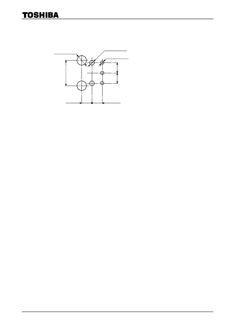
Board Layout Hole Pattern
(for reference)
Unit: mm
Recommended PCB thickness: 1.6 mm
Precautions on Use
(1)
Maximum rating
The maximum ratings are the limit values which must not be exceeded during operation of device. None of
these rating value must not be exceeded. If the maximum rating value is exceeded, the characteristics of
devices may never be restored properly. In extreme cases, the device may be permanently damages.
(2)
Soldering
Optical modules are comprised of internal semiconductor devices. However, in principle, optical modules
are optical components. During soldering, ensure that flux does not contact with the emitting surface or
the detecting surface. Also ensure that proper flux removal is conducted after soldering.
Some optical modules come with a protective cap. The protective cap is used to avoid malfunction when the
optical module is not in use. Note that it is not dust or waterproof.
As mentioned before, optical modules are optical components. Thus, in principle, soldering where there
may be flux residue and flux removal after soldering is not recommended. Toshiba recommend that
soldering be performed without the optical module mounted on the board. Then, after the board has been
cleaned, the optical module should be soldered on to the board manually.
If the optical module cannot be soldered manually, use non-halogen (chlorine-free) flux and make sure,
without cleaning, there is no residue such as chlorine. This is one of the ways to eliminate the effects of
flux. In such a cases, be sure to check the devices' reliability.
(3)
Noise resistance
It is believed that the use of optical transfer devices improve noise resistance. In theory, optical fiber is not
affected by noise at all. However, receiving modules which handle signals whose level is extremely small,
are susceptible to noise.
TOSLINK improve noise resistance to use a conductive case. However, the current signal output by the
optical receiving modules' photodiode is extremely small. Thus, in some environments, shielding the case
may not achieve sufficient noise resistance.
First systems which incorporate TOSLINK, Toshiba recommend testing using the actual device to check its
noise resistance.
Use a simple noise filter on TOSLINK fiber optic transceiving module's power line. If the ripple in the
power supply used is significant, reinforce the filter.
The optical module is to be used in an area which is susceptible to radiated noise, increase the shielding by
covering the optical module and the power line filter with a metallic cover.
(4)
Vibration and shock
This module is plastic sealed and has its wire fixed by resin. This structure is relatively resistant to
vibration and shock. In actual equipment, there are sometime cases in which vibration, shock, or stress is
applied to soldered parts or connected parts, resulting in lines cut. A care must be taken in the design of
equipment which will be subject to high levels of vibration.
2 1.1 0.05
2 1.7 0.05
3 0.8 0.05
5
2
2
2.625 typ.
2.61 typ.
相關(guān)PDF資料 |
PDF描述 |
|---|---|
| TORX170 | FIBER OPTIC RECEIVING MODULE |
| TORX173 | FIBER OPTIC RECEIVING MODULE |
| TORX176 | FIBER OPTIC RECEIVING MODULE FOR DIGITAL AUDIO EQUIPMENT |
| TORX179PL | FIBER OPTIC RECEIVING MODULE |
| TORX180 | FIBER OPTIC RECEIVING MODULE FOR SIMPLEX DIGITAL SIGNAL TRANSMISSION |
相關(guān)代理商/技術(shù)參數(shù) |
參數(shù)描述 |
|---|---|
| TORX141P(F) | 制造商:Toshiba 功能描述:RX 制造商:Toshiba 功能描述:RX Cut Tape |
| TORX141PL | 制造商:Toshiba America Electronic Components 功能描述:RX Optical Fiber 15Mbps 5-Pin |
| TORX141PL(F) | 制造商:Toshiba America Electronic Components 功能描述: |
| TORX142L | 功能描述:RECEIVER MOD FIBER OPTIC W/SHUT RoHS:否 類別:光電元件 >> 光纖 - 接收器 系列:Toslink™ 標(biāo)準(zhǔn)包裝:1 系列:- 數(shù)據(jù)速率:50Mbps 電源電壓:4.75 V ~ 5.25 V 功率 - 最低接收:-22dBm 電流 - 電源:4mA 應(yīng)用:通用 其它名稱:SFH551/1V1SP000063855 |
| TORX142L(F) | 制造商:Toshiba America Electronic Components 功能描述:TX Optical Fiber 125Mbps 3-Pin 制造商:Toshiba 功能描述:Cut Tape 制造商:Toshiba America Electronic Components 功能描述:RECEIVER MOD FIBER OPTIC W/SHUT |
發(fā)布緊急采購,3分鐘左右您將得到回復(fù)。