- 您現(xiàn)在的位置:買賣IC網 > PDF目錄98270 > TPA2005D1GQYRQ1 (TEXAS INSTRUMENTS INC) 1.45 W, 1 CHANNEL, AUDIO AMPLIFIER, PBGA PDF資料下載
參數資料
| 型號: | TPA2005D1GQYRQ1 |
| 廠商: | TEXAS INSTRUMENTS INC |
| 元件分類: | 音頻/視頻放大 |
| 英文描述: | 1.45 W, 1 CHANNEL, AUDIO AMPLIFIER, PBGA |
| 文件頁數: | 29/29頁 |
| 文件大?。?/td> | 1192K |
| 代理商: | TPA2005D1GQYRQ1 |
第1頁第2頁第3頁第4頁第5頁第6頁第7頁第8頁第9頁第10頁第11頁第12頁第13頁第14頁第15頁第16頁第17頁第18頁第19頁第20頁第21頁第22頁第23頁第24頁第25頁第26頁第27頁第28頁當前第29頁
APPLICATION INFORMATION
FULLY DIFFERENTIAL AMPLIFIER
Advantages of Fully Differential Amplifiers
COMPONENT SELECTION
_
+
IN–
IN+
PWM
H–
Bridge
VO+
VO–
Internal
Oscillator
CS
To Battery
VDD
GND
Bias
Circuitry
RI
+
–
Differential
Input
TPA2005D1
Filter-Free Class D
SHUTDOWN
www.ti.com............................................................................................................................................. SLOS474B – AUGUST 2005 – REVISED DECEMBER 2008
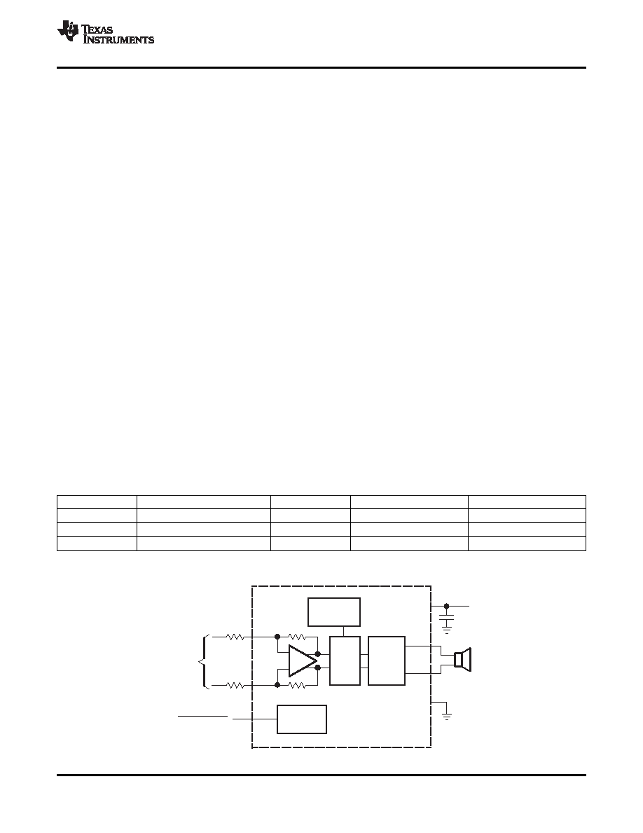
The TPA2005D1 is a fully differential amplifier with differential inputs and outputs. The fully differential amplifier
consists of a differential amplifier and a common-mode amplifier. The differential amplifier ensures that the
amplifier outputs a differential voltage on the output that is equal to the differential input times the gain. The
common-mode feedback ensures that the common-mode voltage at the output is biased around VDD/2,
regardless of the common-mode voltage at the input. The fully differential TPA2005D1 can still be used with a
single-ended input; however, the TPA2005D1 should be used with differential inputs when in a noisy
environment, like a wireless handset, to ensure maximum noise rejection.
Input-coupling capacitors not required:
–
The fully differential amplifier allows the inputs to be biased at a voltage other than mid-supply. For
example, if a codec has a mid-supply lower than the mid-supply of the TPA2005D1, the common-mode
feedback circuit adjusts, and the TPA2005D1 outputs still is biased at mid-supply of the TPA2005D1. The
inputs of the TPA2005D1 can be biased from 0.5 V to VDD – 0.8 V. If the inputs are biased outside of that
range, input-coupling capacitors are required.
Mid-supply bypass capacitor, C
(BYPASS), not required:
–
The fully differential amplifier does not require a bypass capacitor. This is because any shift in the
mid-supply affects both positive and negative channels equally and cancels at the differential output.
Better RF immunity:
–
GSM handsets save power by turning on and shutting off the RF transmitter at a rate of 217 Hz. The
transmitted signal is picked up on input and output traces. The fully differential amplifier cancels the signal
much better than the typical audio amplifier.
Figure 26 shows the TPA2005D1 typical schematic with differential inputs, and Figure 27 shows the TPA2005D1
with differential inputs and input capacitors, and Figure 28 shows the TPA2005D1 with single-ended inputs.
Differential inputs should be used whenever possible, because the single-ended inputs are much more
susceptible to noise.
Table 1. Typical Component Values
REF DES
VALUE
EIA SIZE
MANUFACTURER
PART NUMBER
RI
150 k
(±0.5%)
0402
Panasonic
ERJ2RHD154V
CS
1
F (+22%, –80%)
0402
Murata
GRP155F50J105Z
CI
(1)
3.3 nF (±10%)
0201
Murata
GRP033B10J332K
(1)
CI is needed only for single-ended input or if VICM is not between 0.5 V and VDD – 0.8 V. CI = 3.3 nF (with RI = 150 k) gives a
high-pass corner frequency of 321 Hz.
Figure 26. Typical TPA2005D1 Application Schematic With Differential Input for a Wireless Phone
Copyright 2005–2008, Texas Instruments Incorporated
9
Product Folder Link(s): TPA2005D1-Q1
相關PDF資料 |
PDF描述 |
|---|---|
| TPA2005D1ZQYRQ1 | 1.45 W, 1 CHANNEL, AUDIO AMPLIFIER, PBGA |
| TPA2005D1GQYR | 1.45 W, 1 CHANNEL, AUDIO AMPLIFIER, PBGA15 |
| TPA2005D1DRBR | 1.45 W, 1 CHANNEL, AUDIO AMPLIFIER, PDSO8 |
| TPA2005D1ZQYRG1 | 1.45 W, 1 CHANNEL, AUDIO AMPLIFIER, PBGA15 |
| TPA2005D1ZQYR | 1.45 W, 1 CHANNEL, AUDIO AMPLIFIER, PBGA15 |
相關代理商/技術參數 |
參數描述 |
|---|---|
| TPA2005D1-Q1 | 制造商:TI 制造商全稱:Texas Instruments 功能描述:1.4-W MONO FILTER-FREE CLASS-D AUDIO POWER AMPLIFIER |
| TPA2005D1TDGNRQ1 | 功能描述:音頻放大器 1.4W Mono Fil-Free Class-D Aud Pwr Amp RoHS:否 制造商:STMicroelectronics 產品:General Purpose Audio Amplifiers 輸出類型:Digital 輸出功率: THD + 噪聲: 工作電源電壓:3.3 V 電源電流: 最大功率耗散: 最大工作溫度: 安裝風格:SMD/SMT 封裝 / 箱體:TQFP-64 封裝:Reel |
| TPA2005D1ZQYR | 功能描述:音頻放大器 Mono Fully Diff Filter-Free Class-D RoHS:否 制造商:STMicroelectronics 產品:General Purpose Audio Amplifiers 輸出類型:Digital 輸出功率: THD + 噪聲: 工作電源電壓:3.3 V 電源電流: 最大功率耗散: 最大工作溫度: 安裝風格:SMD/SMT 封裝 / 箱體:TQFP-64 封裝:Reel |
| TPA2005D1ZQYRG1 | 功能描述:音頻放大器 1.4W Mono Class-D Audio Amp RoHS:否 制造商:STMicroelectronics 產品:General Purpose Audio Amplifiers 輸出類型:Digital 輸出功率: THD + 噪聲: 工作電源電壓:3.3 V 電源電流: 最大功率耗散: 最大工作溫度: 安裝風格:SMD/SMT 封裝 / 箱體:TQFP-64 封裝:Reel |
| TPA2006D1 | 制造商:TI 制造商全稱:Texas Instruments 功能描述:1.45-W MONO FILTER-FREE CLASS-D AUDIO POWER AMPLIFIER WITH 1.8-V COMPATIBLE INPUT THRESHOLDS |
發(fā)布緊急采購,3分鐘左右您將得到回復。