- 您現(xiàn)在的位置:買賣IC網(wǎng) > PDF目錄98273 > TPA3107D2PAPR (TEXAS INSTRUMENTS INC) 15 W, 2 CHANNEL, AUDIO AMPLIFIER, PQFP64 PDF資料下載
參數(shù)資料
| 型號: | TPA3107D2PAPR |
| 廠商: | TEXAS INSTRUMENTS INC |
| 元件分類: | 音頻/視頻放大 |
| 英文描述: | 15 W, 2 CHANNEL, AUDIO AMPLIFIER, PQFP64 |
| 封裝: | 10 X 10 MM, GREEN, PLASTIC, HTQFP-64 |
| 文件頁數(shù): | 12/32頁 |
| 文件大小: | 1027K |
| 代理商: | TPA3107D2PAPR |
第1頁第2頁第3頁第4頁第5頁第6頁第7頁第8頁第9頁第10頁第11頁當前第12頁第13頁第14頁第15頁第16頁第17頁第18頁第19頁第20頁第21頁第22頁第23頁第24頁第25頁第26頁第27頁第28頁第29頁第30頁第31頁第32頁

www.ti.com
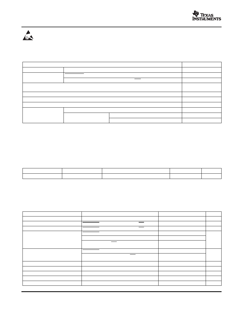
ABSOLUTE MAXIMUM RATINGS
TYPICAL DISSIPATION RATINGS
RECOMMENDED OPERATING CONDITIONS
SLOS509B – OCTOBER 2006 – REVISED JULY 2007
These devices have limited built-in ESD protection. The leads should be shorted together or the device placed in conductive foam
during storage or handling to prevent electrostatic damage to the MOS gates.
over operating free-air temperature range (unless otherwise noted)
(1)
UNIT
VCC
Supply voltage
AVCC, PVCC
–0.3 V to 30 V
SHUTDOWN, MUTE
–0.3 V to VCC + 0.3 V
VI
Input voltage
GAIN0, GAIN1, RINN, RINP, LINN, LINP, MSTR/SLV, SYNC
–0.3 V to VREG + 0.5 V
Continuous total power dissipation
See Dissipation Rating
Table
TA
Operating free-air temperature range
–40
°C to 85°C
TJ
Operating junction temperature range(2)
–40
°C to 150°C
Tstg
Storage temperature range
–65
°C to 150°C
Human body model (3) (all pins)
±2 kV
Electrostatic
All pins except BS pins
±500 V
discharge
Charged-device model (4)
BS Pins – BSLP, BSLN, BSRP, and BSRN
±250 V
(1)
Stresses beyond those listed under absolute maximum ratings may cause permanent damage to the device. These are stress ratings
only, and functional operations of the device at these or any other conditions beyond those indicated under recommended operating
conditions is not implied. Exposure to absolute-maximum-rated conditions for extended periods may affect device reliability.
(2)
The TPA3107D2 incorporates an exposed thermal pad on the underside of the chip. This acts as a heatsink, and it must be connected
to a thermally dissipating plane for proper power dissipation. Failure to do so may result in the device going into thermal protection
shutdown. See TI Technical Briefs SCBA017D and SLUA271 for more information about using the QFN thermal pad. See TI Technical
Briefs SLMA002 for more information about using the HTQFP thermal pad.
(3)
In accordance with JEDEC Standard 22, Test Method A114-B.
(4)
In accordance with JEDEC Standard 22, Test Method C101-A
PACKAGE(1)
TA ≤ 25°C
DERATING FACTOR
TA = 70°C
TA = 85°C
64-pin PAP (HTQFP)
5.43 W
43.5 mW/
°C(2)
3.47 W
2.82 W
(1)
For the most current package and ordering information, see the Package Option Addendum at the end of this document, or see the TI
Web site at www.ti.com.
(2)
This data was taken using a 2 oz trace and copper pad that is soldered directly to a 2-layer high-k PCB (EVM). These are typical values.
See TI Technical Briefs SLMA002 for more information about using the HTQFP thermal pad.
over operating free-air temperature range (unless otherwise noted)
PARAMETER
TEST CONDITIONS
MIN
MAX
UNIT
VCC
Supply voltage
PVCC, AVCC
10
26
V
VIH
High-level input voltage
SHUTDOWN, MUTE, GAIN0, GAIN1, MSTR/SLV, SYNC
2
V
VIL
Low-level input voltage
SHUTDOWN, MUTE, GAIN0, GAIN1, MSTR/SLV, SYNC
0.8
V
SHUTDOWN, VI = VCC, VCC = 24 V
125
MUTE, VI = VCC, VCC = 24 V
75
IIH
High-level input current
A
GAIN0, GAIN1, MSTR/SLV, SYNC, VI = VREG,
2
VCC = 24 V
SHUTDOWN, VI = 0, VCC = 24 V
2
IIL
Low-level input current
A
SYNC, MUTE, GAIN0, GAIN1, MSTR/SLV, VI = 0 V,
1
VCC = 24 V
VOH
High-level output voltage
FAULT, IOH = 1 mA
VREG - 0.6
V
VOL
Low-level output voltage
FAULT, IOL = -1 mA
AGND + 0.4
V
fOSC
Oscillator frequency
ROSC Resistor = 100 k
200
300
kHz
RL
Load Resistance
6
TA
Operating free-air temperature
–40
85
°C
2
相關(guān)PDF資料 |
PDF描述 |
|---|---|
| TPA3107D2PAPT | 15 W, 2 CHANNEL, AUDIO AMPLIFIER, PQFP64 |
| TPA3107D2PAP | 15 W, 2 CHANNEL, AUDIO AMPLIFIER, PQFP64 |
| TPA3107D2PAPRG4 | 15 W, 2 CHANNEL, AUDIO AMPLIFIER, PQFP64 |
| TPA3107D2PAPTG4 | 15 W, 2 CHANNEL, AUDIO AMPLIFIER, PQFP64 |
| TPA3107D2PAPG4 | 15 W, 2 CHANNEL, AUDIO AMPLIFIER, PQFP64 |
相關(guān)代理商/技術(shù)參數(shù) |
參數(shù)描述 |
|---|---|
| TPA3107D2PAPRG4 | 功能描述:音頻放大器 15W Stereo Class-D Audio Power Amp RoHS:否 制造商:STMicroelectronics 產(chǎn)品:General Purpose Audio Amplifiers 輸出類型:Digital 輸出功率: THD + 噪聲: 工作電源電壓:3.3 V 電源電流: 最大功率耗散: 最大工作溫度: 安裝風格:SMD/SMT 封裝 / 箱體:TQFP-64 封裝:Reel |
| TPA3107D2PAPT | 功能描述:音頻放大器 15W Stereo Class-D Audio Power Amp RoHS:否 制造商:STMicroelectronics 產(chǎn)品:General Purpose Audio Amplifiers 輸出類型:Digital 輸出功率: THD + 噪聲: 工作電源電壓:3.3 V 電源電流: 最大功率耗散: 最大工作溫度: 安裝風格:SMD/SMT 封裝 / 箱體:TQFP-64 封裝:Reel |
| TPA3107D2PAPTG4 | 功能描述:音頻放大器 15W Stereo Class-D Audio Power Amp RoHS:否 制造商:STMicroelectronics 產(chǎn)品:General Purpose Audio Amplifiers 輸出類型:Digital 輸出功率: THD + 噪聲: 工作電源電壓:3.3 V 電源電流: 最大功率耗散: 最大工作溫度: 安裝風格:SMD/SMT 封裝 / 箱體:TQFP-64 封裝:Reel |
| TPA311 | 制造商:TI 制造商全稱:Texas Instruments 功能描述:350-mW MONO AUDIO POWER AMPLIFIER |
| TPA311_07 | 制造商:TI 制造商全稱:Texas Instruments 功能描述:350-mW MONO AUDIO POWER AMPLIFIER |
發(fā)布緊急采購,3分鐘左右您將得到回復(fù)。