- 您現(xiàn)在的位置:買賣IC網(wǎng) > PDF目錄98274 > TPA6013A4PWPG4 (TEXAS INSTRUMENTS INC) 2 CHANNEL(S), TONE CONTROL CIRCUIT, PDSO24 PDF資料下載
參數(shù)資料
| 型號(hào): | TPA6013A4PWPG4 |
| 廠商: | TEXAS INSTRUMENTS INC |
| 元件分類: | 音頻控制 |
| 英文描述: | 2 CHANNEL(S), TONE CONTROL CIRCUIT, PDSO24 |
| 封裝: | GREEN, PLASTIC, HTSSOP-24 |
| 文件頁(yè)數(shù): | 11/30頁(yè) |
| 文件大?。?/td> | 743K |
| 代理商: | TPA6013A4PWPG4 |
第1頁(yè)第2頁(yè)第3頁(yè)第4頁(yè)第5頁(yè)第6頁(yè)第7頁(yè)第8頁(yè)第9頁(yè)第10頁(yè)當(dāng)前第11頁(yè)第12頁(yè)第13頁(yè)第14頁(yè)第15頁(yè)第16頁(yè)第17頁(yè)第18頁(yè)第19頁(yè)第20頁(yè)第21頁(yè)第22頁(yè)第23頁(yè)第24頁(yè)第25頁(yè)第26頁(yè)第27頁(yè)第28頁(yè)第29頁(yè)第30頁(yè)
f
c(high) +
1
2 p R
L
C
(C)
3 dB
fc
www.ti.com
SLOS635 – NOVEMBER 2009
POWER SUPPLY DECOUPLING, C(S)
The TPA6013A4 is a high-performance CMOS audio amplifier that requires adequate power supply decoupling to
ensure the output total harmonic distortion (THD) is as low as possible. Power supply decoupling also prevents
oscillations for long lead lengths between the amplifier and the speaker. The optimum decoupling is achieved by
using two capacitors of different types that target different types of noise on the power supply leads. For higher
frequency transients, spikes, or digital hash on the line, a good low equivalent-series-resistance (ESR) ceramic
capacitor, typically 0.1
μF placed as close as possible to the device VDD lead, works best. For filtering
lower-frequency noise signals, a larger aluminum electrolytic capacitor of 10
μF or greater placed near the audio
power amplifier is recommended.
MIDRAIL BYPASS CAPACITOR, C(BYP)
The midrail bypass capacitor (C(BYP)) is the most critical capacitor and serves several important functions. During
start-up or recovery from shutdown mode, C(BYP) determines the rate at which the amplifier starts up. The second
function is to reduce noise produced by the power supply caused by coupling into the output drive signal. This
noise is from the midrail generation circuit internal to the amplifier, which appears as degraded PSRR and
THD+N.
Bypass capacitor (C(BYP)) values of 0.47-μF to 1-μF ceramic or tantalum low-ESR capacitors are recommended
for the best THD and noise performance. For the best pop performance, choose a value for C(BYP) that is equal to
or greater than the value chosen for Ci. This ensures that the input capacitors are charged up to the midrail
voltage before C(BYP) is fully charged to the midrail voltage.
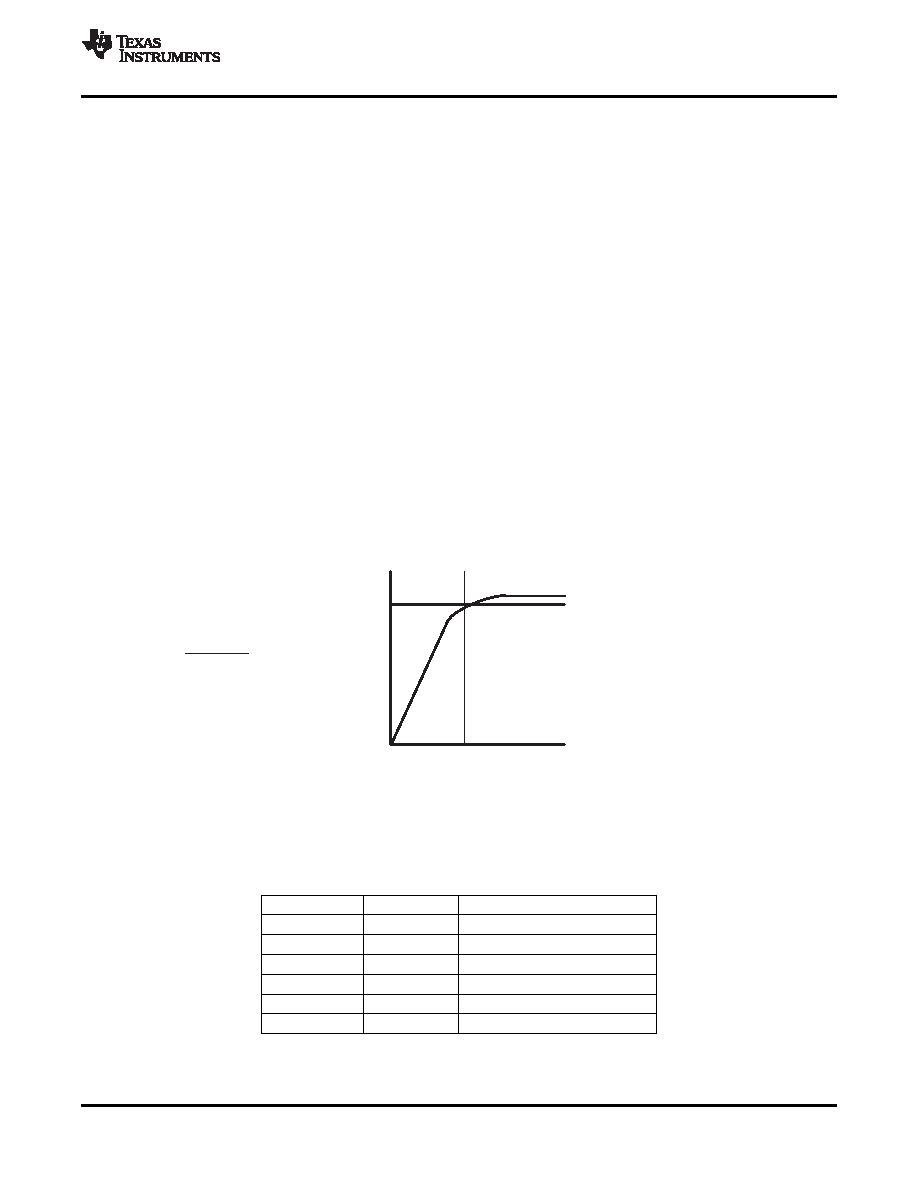
OUTPUT COUPLING CAPACITOR, C(C)
In the typical single-supply SE configuration, an output coupling capacitor (C(C)) is required to block the dc bias at
the output of the amplifier, thus preventing dc currents in the load. As with the input coupling capacitor, the
output coupling capacitor and impedance of the load form a high-pass filter governed by Equation 4.
(4)
The main disadvantage, from a performance standpoint, is the load impedances are typically small, which drives
the low-frequency corner higher, degrading the bass response. Large values of C(C) are required to pass low
frequencies into the load. Consider the example where a C(C) of 330 μF is chosen and loads vary from 3 ,4 ,
8
, 32 , 10 k, and 47 k. Table 4 summarizes the frequency response characteristics of each configuration.
Table 4. Common Load Impedances vs Low Frequency
Output Characteristics in SE Mode
RL
C(C)
LOWEST FREQUENCY
3
330
μF
161 Hz
4
330
μF
120 Hz
8
330
μF
60 Hz
32
330 F
15 Hz
10,000
330
μF
0.05 Hz
47,000
330
μF
0.01 Hz
Copyright 2009, Texas Instruments Incorporated
19
Product Folder Link(s) :TPA6013A4
相關(guān)PDF資料 |
PDF描述 |
|---|---|
| TPA6013A4PWPRG4 | 2 CHANNEL(S), TONE CONTROL CIRCUIT, PDSO24 |
| TPA6017A2PWPR | 1.9 W, 2 CHANNEL, AUDIO AMPLIFIER, PDSO20 |
| TPA6017A2PWP | 1.9 W, 2 CHANNEL, AUDIO AMPLIFIER, PDSO20 |
| TPA6017A2PWPG4 | 1.9 W, 2 CHANNEL, AUDIO AMPLIFIER, PDSO20 |
| TPA6017A2PWPRG4 | 1.9 W, 2 CHANNEL, AUDIO AMPLIFIER, PDSO20 |
相關(guān)代理商/技術(shù)參數(shù) |
參數(shù)描述 |
|---|---|
| TPA6013A4PWPR | 功能描述:音頻放大器 3W Stereo Audio Pwr Amp RoHS:否 制造商:STMicroelectronics 產(chǎn)品:General Purpose Audio Amplifiers 輸出類型:Digital 輸出功率: THD + 噪聲: 工作電源電壓:3.3 V 電源電流: 最大功率耗散: 最大工作溫度: 安裝風(fēng)格:SMD/SMT 封裝 / 箱體:TQFP-64 封裝:Reel |
| TPA6013A4PWPRG4 | 制造商:TI 制造商全稱:Texas Instruments 功能描述:3-W STEREO AUDIO POWER AMPLIFIER WITH ADVANCED DC VOLUME CONTROL |
| TPA6017A2 | 制造商:TI 制造商全稱:Texas Instruments 功能描述:2 W STEREO AUDIO POWER AMPLIFIER WITH FOUR SELECTABLE GAIN SETTINGS |
| TPA6017A2_07 | 制造商:TI 制造商全稱:Texas Instruments 功能描述:2-W STEREO AUDIO POWER AMPLIFIER WITH FOUR SELECTABLE GAIN SETTINGS |
| TPA6017A2_13 | 制造商:TI 制造商全稱:Texas Instruments 功能描述:Introduction and Table of Contents |
發(fā)布緊急采購(gòu),3分鐘左右您將得到回復(fù)。