- 您現(xiàn)在的位置:買賣IC網(wǎng) > PDF目錄98277 > TPD4112KLBR BRUSHLESS DC MOTOR CONTROLLER, 2 A, PZFM23 PDF資料下載
參數(shù)資料
| 型號(hào): | TPD4112KLBR |
| 元件分類: | 運(yùn)動(dòng)控制電子 |
| 英文描述: | BRUSHLESS DC MOTOR CONTROLLER, 2 A, PZFM23 |
| 封裝: | 1.27 MM PITCH, LEAD FREE, PLASTIC, HZIP-23 |
| 文件頁(yè)數(shù): | 4/27頁(yè) |
| 文件大?。?/td> | 391K |
| 代理商: | TPD4112KLBR |
第1頁(yè)第2頁(yè)第3頁(yè)當(dāng)前第4頁(yè)第5頁(yè)第6頁(yè)第7頁(yè)第8頁(yè)第9頁(yè)第10頁(yè)第11頁(yè)第12頁(yè)第13頁(yè)第14頁(yè)第15頁(yè)第16頁(yè)第17頁(yè)第18頁(yè)第19頁(yè)第20頁(yè)第21頁(yè)第22頁(yè)第23頁(yè)第24頁(yè)第25頁(yè)第26頁(yè)第27頁(yè)
TPD4112K
2006-06-30
12
Description of Bootstrap Capacitor Charging and Its Capacitance
The IC uses bootstrapping for the power supply for high-side drivers.
The bootstrap capacitor is charged by turning on the low-side IGBT of the same arm (approximately 1/5 of PWM
cycle) while the high-side IGBT controlled by PWM is off. (For example, to drive at 20 kHz, it takes approximately
10 ms per cycle to charge the capacitor.) When the VS voltage exceeds 3.8 V (55% duty), the low-side IGBT is
continuously in the off state. This is because when the PWM on-duty becomes larger, the arm is short-circuited
while the low-side IGBT is on. Even in this state, because PWM control is being performed on the high-side IGBT,
the regenerative current of the diode flows to the low-side FRD of the same arm, and the bootstrap capacitor is
charged. Note that when the on-duty is 100%, diode regenerative current does not flow; thus, the bootstrap
capacitor is not charged.
When driving a motor at 100 % duty cycle, take the voltage drop at 100% duty (see the figure below) into
consideration to determine the capacitance of the bootstrap capacitor.
Capacitance of the bootstrap capacitor
= Consumption current (max) of the high-side driver × Maximum drive time
/(VCC VF (BSD) + VF (FRD) 13.5) [F]
VF (BSD) : Bootstrap diode forward voltage
VF (FRD) : Flywheel diode forward voltage
Consideration must be made for aging and temperature change of the capacitor.
VS Range
IGBT Operation
A
Both high- and low-side OFF.
B
Charging range. Low-side IGBT refreshing on the phase the high-side IGBT in PWM.
C
No charging range. High-side at PWM according to the timing chart. Low-side no refreshing.
Safe Operating Area
Note 1: The above safe operating areas are at Tj
= 135°C (Figure 1) and Tc = 95°C (Figure 2). If the temperature
exceeds these, the safe operation areas are reduced.
Note 2: The above safe operating areas include the over-current protection operation area.
1.0
0
400
Peak
winding
current
(A)
Power supply voltage VBB (V)
Figure 1 SOA at Tj
= 135°C
0
1.1
0
400
Peak
winding
current
(A)
Power supply voltage VBB (V)
Figure 2 SOA at Tc
= 95°C
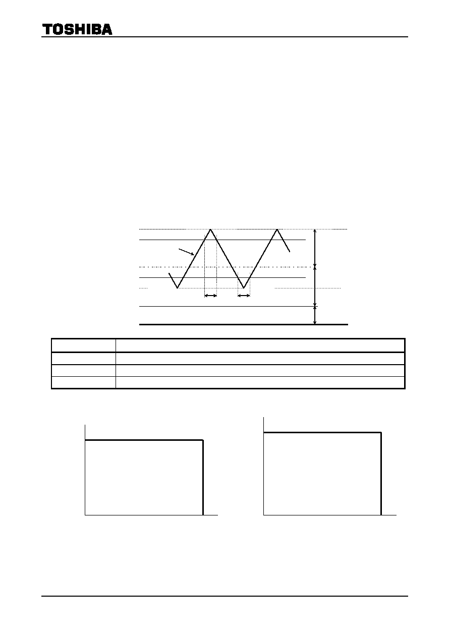
0
Low-side ON
Duty cycle 80%
C
Triangular wave
Duty cycle 100% (VS: 5.4 V)
High-side duty ON
PWM reference voltage
Duty cyle 55% (VS: 3.8 V)
Duty cycle 0% (VS: 2.1 V)
VVsOFF (VS: 1.3 V)
GND
B
A
相關(guān)PDF資料 |
PDF描述 |
|---|---|
| TPD4112K | BRUSHLESS DC MOTOR CONTROLLER, PZFM23 |
| TPD4113AKLB2 | BRUSHLESS DC MOTOR CONTROLLER, 1 A, PZFM23 |
| TPD4124AK | BRUSHLESS DC MOTOR CONTROLLER, 3 A, PDIP26 |
| TPD4125AK | BRUSHLESS DC MOTOR CONTROLLER, 4 A, PDIP26 |
| TPD4131K | BRUSHLESS DC MOTOR CONTROLLER, PDIP26 |
相關(guān)代理商/技術(shù)參數(shù) |
參數(shù)描述 |
|---|---|
| TPD4113AK | 制造商:TOSHIBA 制造商全稱:Toshiba Semiconductor 功能描述:High Voltage Monolithic Silicon Power IC |
| TPD4113AK(LB2,Q) | 制造商:Toshiba America Electronic Components 功能描述: |
| TPD4113AK_07 | 制造商:TOSHIBA 制造商全稱:Toshiba Semiconductor 功能描述:High Voltage Monolithic Silicon Power IC |
| TPD4113K | 制造商:TOSHIBA 制造商全稱:Toshiba Semiconductor 功能描述:High Voltage Monolithic Silicon Power IC |
| TPD4113K_07 | 制造商:TOSHIBA 制造商全稱:Toshiba Semiconductor 功能描述:High Voltage Monolithic Silicon Power IC |
發(fā)布緊急采購(gòu),3分鐘左右您將得到回復(fù)。