- 您現(xiàn)在的位置:買賣IC網(wǎng) > PDF目錄68612 > TPS2211APW (TEXAS INSTRUMENTS INC) 3-CHANNEL POWER SUPPLY SUPPORT CKT, PDSO20 PDF資料下載
參數(shù)資料
| 型號: | TPS2211APW |
| 廠商: | TEXAS INSTRUMENTS INC |
| 元件分類: | 電源管理 |
| 英文描述: | 3-CHANNEL POWER SUPPLY SUPPORT CKT, PDSO20 |
| 封裝: | GREEN, PLASTIC, TSSOP-20 |
| 文件頁數(shù): | 19/25頁 |
| 文件大?。?/td> | 580K |
| 代理商: | TPS2211APW |
TPS2211A
SINGLESLOT PC CARD POWER INTERFACE SWITCH
FOR PARALLEL PCMCIA CONTROLLERS
SLVS282B SEPTEMBER 2000 REVISED JULY 2005
3
WWW.TI.COM
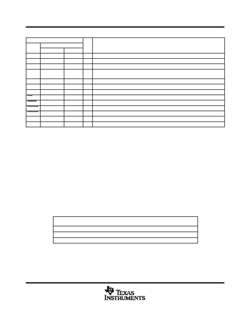
Terminal Functions
TERMINAL
NAME
NO.
I/O
DESCRIPTION
NAME
PW, PWP
DB
I/O
DESCRIPTION
3.3V
3, 4
I
3.3-V VCC input for card power and/or chip power if 5 V is not present
5V
5, 6
I
5-V VCC input for card power and/or chip power
12V
10
9
I
12-V Vpp input card power
AVCC
13, 14, 15, 16
11, 12, 13
O
Switched output that delivers 0 V, 3.3-V, 5-V, or high impedance to card; must be tied together
externally for the 20-pin PWP package.
AVPP
11
10
O
Switched output that delivers 0 V, 3.3-V, 5-V, 12-V, or high impedance to card
GND
8
7
Ground
NC
7, 12, 17
No internal connection
OC
9
8
O
Logic-level overcurrent reporting output that goes low when an overcurrent conditions exists
SHDN
20
16
I
Logic input that shuts down the device and sets all power outputs to high-impedance state
VCCD0
1
I
Logic input that controls voltage of AVCC (see control-logic table)
VCCD1
2
I
Logic input that controls voltage of AVCC (see control-logic table)
VPPD0
19
15
I
Logic input that controls voltage of AVPP (see control-logic table)
VPPD1
18
14
I
Logic input that controls voltage of AVPP (see control-logic table)
absolute maximum ratings over operating free-air temperature (unless otherwise noted)
Input voltage range for card power:
VI(5V)
0.3 V to 7 V
. . . . . . . . . . . . . . . . . . . . . . . . . . . . . . . . . . . . . . . . . . .
VI(3.3V)
0.3 V to 7 V
. . . . . . . . . . . . . . . . . . . . . . . . . . . . . . . . . . . . . . . . .
VI(12V)
0.3 V to 14 V
. . . . . . . . . . . . . . . . . . . . . . . . . . . . . . . . . . . . . . . . .
Logic input voltage
0.3 V to 7 V
. . . . . . . . . . . . . . . . . . . . . . . . . . . . . . . . . . . . . . . . . . . . . . . . . . . . . . . . . . . . . . . . .
Continuous total power dissipation
See Dissipation Rating Table
. . . . . . . . . . . . . . . . . . . . . . . . . . . . . . . . . . . . .
Output current (each card):
IO(VCC)
internally limited
. . . . . . . . . . . . . . . . . . . . . . . . . . . . . . . . . . . . . . . . . . . . . .
IO(VPP)
internally limited
. . . . . . . . . . . . . . . . . . . . . . . . . . . . . . . . . . . . . . . . . . . . . .
Operating virtual junction temperature range, TJ
40
°C to 150°C
. . . . . . . . . . . . . . . . . . . . . . . . . . . . . . . . . . . . .
Operating free-air temperature range, TA
40
°C to 85°C
. . . . . . . . . . . . . . . . . . . . . . . . . . . . . . . . . . . . . . . . . . . .
Storage temperature range, Tstg
55
°C to 150°C
. . . . . . . . . . . . . . . . . . . . . . . . . . . . . . . . . . . . . . . . . . . . . . . . . . .
Lead temperature 1,6 mm (1/16 inch) from case for 10 seconds
260
°C
. . . . . . . . . . . . . . . . . . . . . . . . . . . . . . .
Stresses beyond those listed under “absolute maximum ratings” may cause permanent damage to the device. These are stress ratings only, and
functional operation of the device at these or any other conditions beyond those indicated under “recommended operating conditions” is not
implied. Exposure to absolute-maximum-rated conditions for extended periods may affect device reliability.
DISSIPATION RATING TABLE
PACKAGE
TA ≤ 25°C
POWER RATING
DERATING FACTOR
ABOVE TA = 25°C
TA = 70°C
POWER RATING
TA = 85°C
POWER RATING
DB16
800 mW
8.0 mW/
°C
440 mW
320 mW
PW20
741.3 mW
7.41 mW/
°C
407.7 mW
296.5 mW
PWP20
2740 mW
27.4 mW/
°C
1507 mW
1096 mW
These devices are mounted on a Low-K PCB with 0 LFM.
相關(guān)PDF資料 |
PDF描述 |
|---|---|
| TPS2211APWG4 | 3-CHANNEL POWER SUPPLY SUPPORT CKT, PDSO20 |
| TPS2211APWR | 3-CHANNEL POWER SUPPLY SUPPORT CKT, PDSO20 |
| TPS2211AIDBR | 3-CHANNEL POWER SUPPLY SUPPORT CKT, PDSO16 |
| TPS22921YZPR | 1-CHANNEL POWER SUPPLY SUPPORT CKT, BGA6 |
| TPS22922BYFPR | 1-CHANNEL POWER SUPPLY SUPPORT CKT, BGA6 |
相關(guān)代理商/技術(shù)參數(shù) |
參數(shù)描述 |
|---|---|
| TPS2211APWG4 | 功能描述:熱插拔功率分布 1A Sngl-Slot PC Card Power Switch RoHS:否 制造商:Texas Instruments 產(chǎn)品:Controllers & Switches 電流限制: 電源電壓-最大:7 V 電源電壓-最小:- 0.3 V 工作溫度范圍: 功率耗散: 安裝風(fēng)格:SMD/SMT 封裝 / 箱體:MSOP-8 封裝:Tube |
| TPS2211APWP | 功能描述:熱插拔功率分布 PCMCIA Pwr Intfce Sw RoHS:否 制造商:Texas Instruments 產(chǎn)品:Controllers & Switches 電流限制: 電源電壓-最大:7 V 電源電壓-最小:- 0.3 V 工作溫度范圍: 功率耗散: 安裝風(fēng)格:SMD/SMT 封裝 / 箱體:MSOP-8 封裝:Tube |
| TPS2211APWPG4 | 功能描述:熱插拔功率分布 1A Sngl-Slot PC Card Power Switch RoHS:否 制造商:Texas Instruments 產(chǎn)品:Controllers & Switches 電流限制: 電源電壓-最大:7 V 電源電壓-最小:- 0.3 V 工作溫度范圍: 功率耗散: 安裝風(fēng)格:SMD/SMT 封裝 / 箱體:MSOP-8 封裝:Tube |
| TPS2211APWPR | 功能描述:熱插拔功率分布 1A Sngl-Slot PC Card Power Switch RoHS:否 制造商:Texas Instruments 產(chǎn)品:Controllers & Switches 電流限制: 電源電壓-最大:7 V 電源電壓-最小:- 0.3 V 工作溫度范圍: 功率耗散: 安裝風(fēng)格:SMD/SMT 封裝 / 箱體:MSOP-8 封裝:Tube |
| TPS2211APWPRG4 | 功能描述:熱插拔功率分布 1A Sngl-Slot PC Card Power Switch RoHS:否 制造商:Texas Instruments 產(chǎn)品:Controllers & Switches 電流限制: 電源電壓-最大:7 V 電源電壓-最小:- 0.3 V 工作溫度范圍: 功率耗散: 安裝風(fēng)格:SMD/SMT 封裝 / 箱體:MSOP-8 封裝:Tube |
發(fā)布緊急采購,3分鐘左右您將得到回復(fù)。