- 您現(xiàn)在的位置:買賣IC網(wǎng) > PDF目錄231084 > TPS40055PWP (TEXAS INSTRUMENTS INC) SWITCHING CONTROLLER, 1000 kHz SWITCHING FREQ-MAX, PDSO16 PDF資料下載
參數(shù)資料
| 型號: | TPS40055PWP |
| 廠商: | TEXAS INSTRUMENTS INC |
| 元件分類: | 穩(wěn)壓器 |
| 英文描述: | SWITCHING CONTROLLER, 1000 kHz SWITCHING FREQ-MAX, PDSO16 |
| 封裝: | GREEN, PLASTIC, HTSSOP-16 |
| 文件頁數(shù): | 31/35頁 |
| 文件大小: | 866K |
| 代理商: | TPS40055PWP |
第1頁第2頁第3頁第4頁第5頁第6頁第7頁第8頁第9頁第10頁第11頁第12頁第13頁第14頁第15頁第16頁第17頁第18頁第19頁第20頁第21頁第22頁第23頁第24頁第25頁第26頁第27頁第28頁第29頁第30頁當(dāng)前第31頁第32頁第33頁第34頁第35頁
1
2
3
4
5
6
7
8
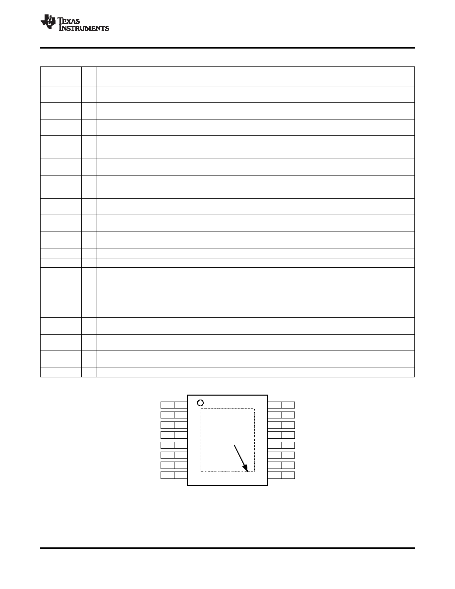
16
15
14
13
12
11
10
9
ILIM
VIN
BOOST
HDRV
SW
BP10
LDRV
PGND
KFF
RT
BP5
SYNC
SGND
SS/SD
VFB
COMP
Thermal Pad
www.ti.com ...................................................................................................................................... SLUS593F – DECEMBER 2003 – REVISED SEPTEMBER 2008
Table 1. PIN DESCRIPTIONS
TERMINAL
I/O
DESCRIPTION
NAME
NO.
Gate drive voltage for the high side N-channel MOSFET. The BOOST voltage is 9 V greater than the SW voltage. A
BOOST
14
O
0.1-F ceramic capacitor should be connected from this pin to the drain of the lower MOSFET.
5-V reference. This pin should be bypassed to ground with a 0.1-F ceramic capacitor. This pin may be used with an
BP5
3
O
external DC load of 1 mA or less.
10-V reference used for gate drive of the N-channel synchronous rectifier. This pin should be bypassed by a 1-F
BP10
11
O
ceramic capacitor. This pin may be used with an external DC load of 1 mA or less.
Output of the error amplifier, input to the PWM comparator. A feedback network is connected from this pin to the VFB
COMP
8
O
pin to compensate the overall loop. The comp pin is internally clamped above the peak of the ramp to improve large
signal transient response.
Floating gate drive for the high-side N-channel MOSFET. This pin switches from BOOST (MOSFET on) to SW
HDRV
13
O
(MOSFET off).
Current limit pin, used to set the overcurrent threshold. An internal current sink from this pin to ground sets a voltage
ILIM
16
I
drop across an external resistor connected from this pin to VCC. The voltage on this pin is compared to the voltage
drop (VIN – SW) across the high-side MOSFET during conduction.
A resistor is connected from this pin to VIN to program the amount of voltage feed-forward and UVLO level. The
KFF
1
I
current fed into this pin is internally divided and used to control the slope of the PWM ramp.
Gate drive for the N-channel synchronous rectifier. This pin switches from BP10 (MOSFET on) to ground (MOSFET
LDRV
10
O
off).
Power ground reference for the device. There should be a low-impedance path from this pin to the source(s) of the
PGND
9
lower MOSFET(s).
RT
2
I
A resistor is connected from this pin to ground to set the internal oscillator and switching frequency.
SGND
5
Signal ground reference for the device.
Soft-start programming and shutdown pin. A capacitor connected from this pin to ground programs the soft-start time.
The capacitor is charged with an internal current source of 2.3 A. The resulting voltage ramp on the SS/SD pin is
used as a second non-inverting input to the error amplifier. The output voltage begins to rise when VSS/SD is
SS/SD
6
I
approximately 0.85 V. The output continues to rise and reaches regulation when VSS/SD is approximately 1.55 V. The
controller is considered shut down when VSS/SD is 125 mV or less. The internal circuitry is enabled when VSS/SD is 210
mV or greater. When VSS/SD is less than approximately 0.85 V, the outputs cease switching and the output voltage
(VO) decays while the internal circuitry remains active.
This pin is connected to the switched node of the converter and used for overcurrent sensing. The TPS40054 also
SW
12
I
uses this pin for zero current sensing.
Syncronization input for the device. This pin can be used to synchronize the oscillator to an external master frequency.
SYNC
4
I
If synchronization is not used, connect this pin to SGND.
Inverting input to the error amplifier. In normal operation the voltage on this pin is equal to the internal reference
VFB
7
I
voltage, 0.7 V.
VIN
15
I
Supply voltage for the device.
PWP PACKAGE (TOP VIEW)
A.
For more information on the PWP package, refer to TI Technical Brief, Literature No. SLMA002.
B.
PowerPAD heat slug must be connected to SGND (pin 5) or electrically isolated from all other pins.
Copyright 2003–2008, Texas Instruments Incorporated
5
Product Folder Link(s): TPS40054 TPS40055 TPS40057
相關(guān)PDF資料 |
PDF描述 |
|---|---|
| TPS3824-30DBVRG4 | 1-CHANNEL POWER SUPPLY MANAGEMENT CKT, PDSO5 |
| TPS2300IPWG4 | 2-CHANNEL POWER SUPPLY SUPPORT CKT, PDSO20 |
| TC151A2013EOA723 | 0.25 A SWITCHING REGULATOR, 50 kHz SWITCHING FREQ-MAX, PDSO8 |
| TC151A6022EOA713 | 0.25 A SWITCHING REGULATOR, 50 kHz SWITCHING FREQ-MAX, PDSO8 |
| TC151A1526EOA713 | 0.25 A SWITCHING REGULATOR, 50 kHz SWITCHING FREQ-MAX, PDSO8 |
相關(guān)代理商/技術(shù)參數(shù) |
參數(shù)描述 |
|---|---|
| TPS40055PWPG4 | 功能描述:DC/DC 開關(guān)控制器 Wide Input Sync Buck Cntrlr source/sink RoHS:否 制造商:Texas Instruments 輸入電壓:6 V to 100 V 開關(guān)頻率: 輸出電壓:1.215 V to 80 V 輸出電流:3.5 A 輸出端數(shù)量:1 最大工作溫度:+ 125 C 安裝風(fēng)格: 封裝 / 箱體:CPAK |
| TPS40055PWPR | 功能描述:DC/DC 開關(guān)控制器 Wide Input Sync Buck Cntrlr source/sink RoHS:否 制造商:Texas Instruments 輸入電壓:6 V to 100 V 開關(guān)頻率: 輸出電壓:1.215 V to 80 V 輸出電流:3.5 A 輸出端數(shù)量:1 最大工作溫度:+ 125 C 安裝風(fēng)格: 封裝 / 箱體:CPAK |
| TPS40055PWPRG4 | 功能描述:DC/DC 開關(guān)控制器 Wide Input Sync Buck Cntrlr source/sink RoHS:否 制造商:Texas Instruments 輸入電壓:6 V to 100 V 開關(guān)頻率: 輸出電壓:1.215 V to 80 V 輸出電流:3.5 A 輸出端數(shù)量:1 最大工作溫度:+ 125 C 安裝風(fēng)格: 封裝 / 箱體:CPAK |
| TPS40056 | 制造商:TI 制造商全稱:Texas Instruments 功能描述:WIDE-INPUT SYNCHRONOUS, TRACKING BUCK CONTROLLER |
| TPS40056PWP | 功能描述:DC/DC 開關(guān)控制器 Wide Vin Synch Buck DC/DC Cntrlr RoHS:否 制造商:Texas Instruments 輸入電壓:6 V to 100 V 開關(guān)頻率: 輸出電壓:1.215 V to 80 V 輸出電流:3.5 A 輸出端數(shù)量:1 最大工作溫度:+ 125 C 安裝風(fēng)格: 封裝 / 箱體:CPAK |
發(fā)布緊急采購,3分鐘左右您將得到回復(fù)。