- 您現(xiàn)在的位置:買賣IC網(wǎng) > PDF目錄383963 > TPS5100PW (Texas Instruments, Inc.) TRIPLE-CHANNEL PWM CONTROL CIRCUITS PDF資料下載
參數(shù)資料
| 型號: | TPS5100PW |
| 廠商: | Texas Instruments, Inc. |
| 英文描述: | TRIPLE-CHANNEL PWM CONTROL CIRCUITS |
| 中文描述: | 三通道PWM控制電路 |
| 文件頁數(shù): | 1/11頁 |
| 文件大?。?/td> | 165K |
| 代理商: | TPS5100PW |
TPS5100
TRIPLE-CHANNEL PWMCONTROL CIRCUITS
SLVS169 – JANUARY 2000
1
POST OFFICE BOX 655303
DALLAS, TEXAS 75265
Low Voltage Operation . . . 2.5 V to 7 V
Low Power . . . 3. 5 mA
(f = 500 kHz, Duty = 50%)
Internal Undervoltage Lockout Protection
Internal Short Circuit Protection
Wide Operating Frequency . . . 50 kHz to
1 MHz
Internal Precision Reference . . . 1.25 V
±
1%
(25
°
C)
On/Off Switch for CH1/3 Pair and Ch2 (see
Function Table)
0 to 100% Dead Time Control
Totem Pole Output Stage
Smal l Package . . . 16 Pin TSSOP
description
The TPS5100 is a triple PWM control circuit, primarily designed to compose the power supply for LCD display.
Each PWM channel has own error amplifier, PWM comparator, dead-time control and output driver. The
trimmed voltage reference, oscillator, undervoltage lockout and short circuit protection are common for all
channels.
This device includes two boost exclusive circuits (ch1,3) and a buck-boost exclusive circuit (ch2). The operating
frequency is set with external resister and capacitor, and dead time is continuously adjustable form 0% to 100%
duty cycle with resistive divider network. Soft start function can be implemented by adding a capacitor to dead
time divider network. Two dead time control inputs are assigned for ch1,3 pair and ch2 individually and each
dead time control input can be used to control on/off operation. TPS5100 can operate from 2.5 V supply voltage
and ch1,3 pair and ch2 operate with reverse phase switching each other to achieve efficient operation in low
power and battery powered system.
The TPS5100 is characterized for operation from –20
°
C to 85
°
C.
FUNCTION TABLE
CONDITION
OUTPUT
CH-1
CH-2
CH-3
DTC1/3 >. 0.3 V, DTC2 > 0.3 V
ON H
ON L
ON H
DTC1/3 > 0.3 V, DTC2 <. 0.2 V
ON H
OFF H
ON H
DTC1/3 < 0.2 V, DTC2 > 0.3 V
OFF L
ON L
OFF L
DTC1/3 < 0.2 V, DTC2 < 0.2 V
OFF L
OFF H
OFF L
AVAILABLE OPTIONS
PACKAGE
TSSOP
(PW)
TA
–20
°
C to 85
°
C
TPS5100PW
Copyright
2000, Texas Instruments Incorporated
PRODUCTION DATA information is current as of publication date.
Products conform to specifications per the terms of Texas Instruments
standard warranty. Production processing does not necessarily include
testing of all parameters.
Please be aware that an important notice concerning availability, standard warranty, and use in critical applications of
Texas Instruments semiconductor products and disclaimers thereto appears at the end of this data sheet.
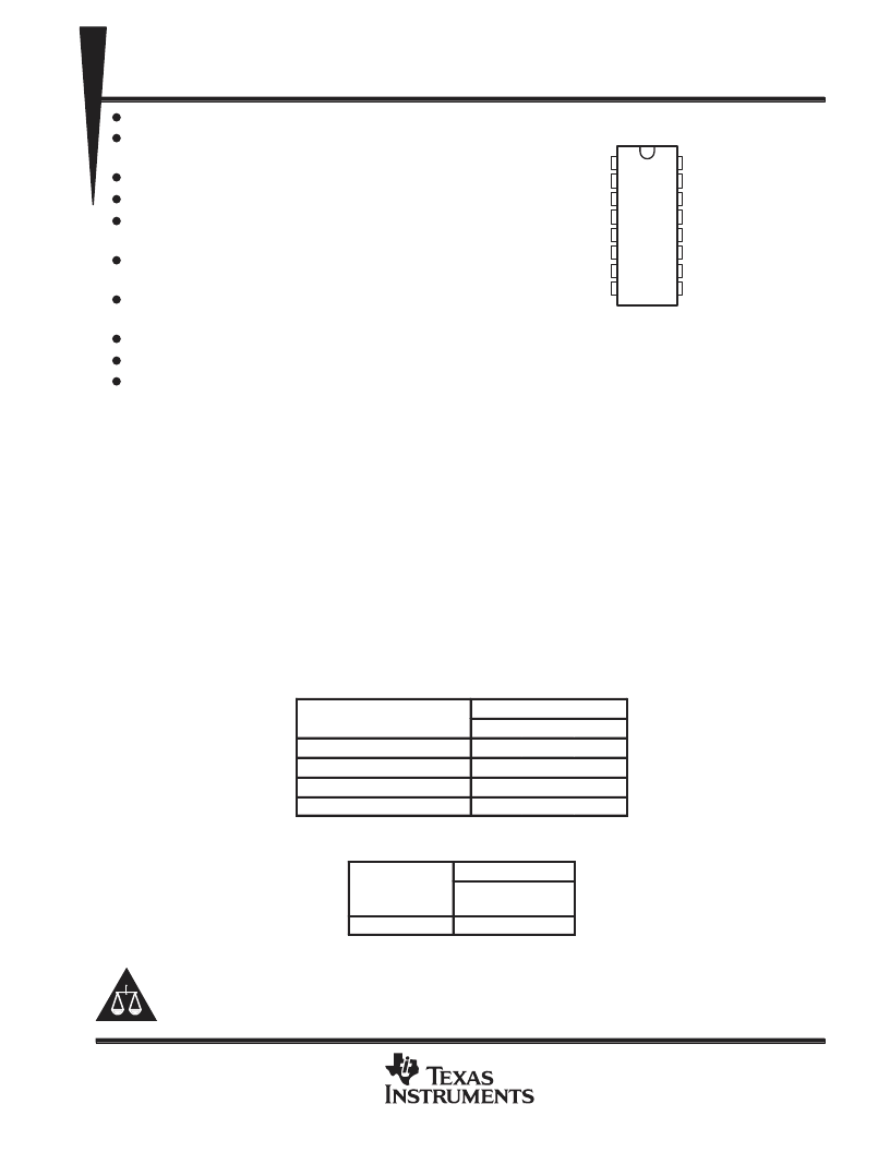
1
2
3
4
5
6
7
8
16
15
14
13
12
11
10
9
IN-2
E/O2
V
CC
OUT2
OUT3
OUT1
GND
SCP
E/O3
IN-3
IN-1
E/O1
C
T
/R
T
DTC2
DTC1/3
V
REF
PW PACKAGE
(TOP VIEW)
相關PDF資料 |
PDF描述 |
|---|---|
| TPS5102DBT | DUAL, HIGH-EFFICIENCY CONTROLLER FOR NOTEBOOK PC POWER |
| TPS5211 | HIGH FREQUENCY PROGRAMMABLE HYSTERETIC REGULATOR CONTROLLER |
| TPS5211PWP | HIGH FREQUENCY PROGRAMMABLE HYSTERETIC REGULATOR CONTROLLER |
| TPS60251RTW | HIGH EFFICIENCY CHARGE PUMP FOR 7 WLEDs WITH I2C INTERFACE |
| TPS61026DRC | 96% EFFICIENT SYNCHRONOUS BOOST CONVERTER |
相關代理商/技術參數(shù) |
參數(shù)描述 |
|---|---|
| TPS5102 | 制造商:TI 制造商全稱:Texas Instruments 功能描述:DUAL, HIGH-EFFICIENCY CONTROLLER FOR NOTEBOOK PC POWER |
| TPS5102_08 | 制造商:TI 制造商全稱:Texas Instruments 功能描述:DUAL, HIGH-EFFICIENCY CONTROLLER FOR NOTEBOOK PC POWER |
| TPS51020 | 制造商:TI 制造商全稱:Texas Instruments 功能描述:DUAL, VOLTAGE MODE, DDR SELECTABLE, SYNCHRONOUS, STEP-DOWN CONTROLLER FOR NOTEBOOK SYSTEM POWER |
| TPS51020DBT | 功能描述:DC/DC 開關控制器 Dual DDR selectable Sync buck Controller RoHS:否 制造商:Texas Instruments 輸入電壓:6 V to 100 V 開關頻率: 輸出電壓:1.215 V to 80 V 輸出電流:3.5 A 輸出端數(shù)量:1 最大工作溫度:+ 125 C 安裝風格: 封裝 / 箱體:CPAK |
| TPS51020DBT | 制造商:Texas Instruments 功能描述:; Leaded Process Compatible:Yes; Peak Re |
發(fā)布緊急采購,3分鐘左右您將得到回復。