- 您現(xiàn)在的位置:買賣IC網(wǎng) > PDF目錄98282 > TPS54320RHLR (TEXAS INSTRUMENTS INC) SWITCHING REGULATOR, 1320 kHz SWITCHING FREQ-MAX, PQCC14 PDF資料下載
參數(shù)資料
| 型號: | TPS54320RHLR |
| 廠商: | TEXAS INSTRUMENTS INC |
| 元件分類: | 穩(wěn)壓器 |
| 英文描述: | SWITCHING REGULATOR, 1320 kHz SWITCHING FREQ-MAX, PQCC14 |
| 封裝: | 3.50 X 3.50 MM, GREEN, PLASTIC, QFN-14 |
| 文件頁數(shù): | 24/39頁 |
| 文件大小: | 1358K |
| 代理商: | TPS54320RHLR |
第1頁第2頁第3頁第4頁第5頁第6頁第7頁第8頁第9頁第10頁第11頁第12頁第13頁第14頁第15頁第16頁第17頁第18頁第19頁第20頁第21頁第22頁第23頁當(dāng)前第24頁第25頁第26頁第27頁第28頁第29頁第30頁第31頁第32頁第33頁第34頁第35頁第36頁第37頁第38頁第39頁
SLVS982A – AUGUST 2010 – REVISED SEPTEMBER 2010
www.ti.com
Bill of Materials
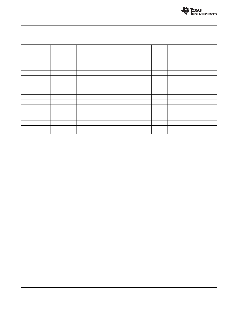
Table 1. Bill of Materials
Count
RefDes
Value
Description
Size
Part Number
MFR
2
C2, C3
4.7 F
Capacitor, Ceramic, 25V, X5R, 10%
0805
Std
1
C4
0.015 F
Capacitor, Ceramic, 50V, X7R, 10%
0603
Std
1
C5
0.1 F
Capacitor, Ceramic, 16V, X7R, 10%
0603
Std
1
C6
330 pF
Capacitor, Ceramic, 25V, X7R, 10%
0603
Std
1
C7
0.01 F
Capacitor, Ceramic, 25V, X7R, 10%
0603
Std
1
C9
47 F
Capacitor, Ceramic, 6.3V, X5R, 20%
1210
Std
1
C11
100 pF
Capacitor, Ceramic, 50V, C0G, 5%
0603
Std
1
L1
6.8 H
Inductor, SMT, 3.6A, 24 milliohm
8.7 mm x
VLP8040T-6R8M
TDK
8.6 mm
1
R1
511K
Resistor, Chip, 1/16W, 1%
0603
Std
2
R2, R3
100K
Resistor, Chip, 1/16W, 1%
0603
Std
1
R4
1.78K
Resistor, Chip, 1/16W, 1%
0603
Std
1
R7
51.1
Resistor, Chip, 1/16W, 1%
0603
Std
1
R8
31.6K
Resistor, Chip, 1/16W, 1%
0603
Std
1
R9
10.0K
Resistor, Chip, 1/16W, 1%
0603
Std
1
U1
TPS54320RHL
IC, 17V Input, 3A Output, Sync. Step Down Switcher QFN14
TPS54320RHL
TI
w/ Integrated FET
PCB Layout Guidelines
Layout is a critical portion of good power supply design. See Figure 56 for a PCB layout example. The top layer
contains the main power traces for VIN, VOUT, and the PH node. Also on the top layer are connections for the
remaining pins of the TPS54320 and a large top side area filled with ground. The top layer ground area should
be connected to the internal ground layer(s) using vias at the input bypass capacitor, the output filter capacitor
and directly under the TPS54320 device to provide a thermal path from the exposed thermal pad land to ground.
The GND pin should be tied directly to the exposed thermal pad under the IC. For operation at full rated load, the
top side ground area together with the internal ground plane, must provide adequate heat dissipating area. There
are several signals paths that conduct fast changing currents or voltages that can interact with stray inductance
or parasitic capacitance to generate noise or degrade the power supplies performance. To help eliminate these
problems, the PVIN pin should be bypassed to ground with a low ESR ceramic bypass capacitor with X5R or
X7R dielectric. Care should be taken to minimize the loop area formed by the bypass capacitor connections, the
PVIN pins, and the ground connections. The VIN pin must also be bypassed to ground using a low ESR ceramic
capacitor with X5R or X7R dielectric. Make sure to connect this capacitor to the quiet analog ground trace rather
than the power ground trace of the PVIN bypass capacitor. Since the PH connection is the switching node, the
output inductor should be located close to the PH pins, and the area of the PCB conductor minimized to prevent
excessive capacitive coupling. The output filter capacitor ground should use the same power ground trace as the
PVIN input bypass capacitor. Try to minimize this conductor length while maintaining adequate width. The small
signal components should be grounded to the analog ground path as shown. The RT/CLK pin is sensitive to
noise so the RT resistor should be located as close as possible to the IC and routed with minimal lengths of
trace. The additional external components can be placed approximately as shown. It may be possible to obtain
acceptable performance with alternate PCB layouts. However, this layout has been shown to produce good
results and is meant as a guideline.
30
Copyright 2010, Texas Instruments Incorporated
Product Folder Link(s) :TPS54320
相關(guān)PDF資料 |
PDF描述 |
|---|---|
| TPS54320RHL | SWITCHING REGULATOR, PQCC14 |
| TPS54327DDAR | 5.7 A SWITCHING REGULATOR, 700 kHz SWITCHING FREQ-MAX, PDSO8 |
| TPS54328DDA | 5.7 A SWITCHING REGULATOR, 700 kHz SWITCHING FREQ-MAX, PDSO8 |
| TPS54328DDAR | 5.7 A SWITCHING REGULATOR, 700 kHz SWITCHING FREQ-MAX, PDSO8 |
| TPS54331DG4 | 2 A SWITCHING REGULATOR, 684 kHz SWITCHING FREQ-MAX, PDSO8 |
相關(guān)代理商/技術(shù)參數(shù) |
參數(shù)描述 |
|---|---|
| TPS54320RHLT | 功能描述:直流/直流開關(guān)調(diào)節(jié)器 4.5-17V Inp3A Sync Step Down Cnvrtr RoHS:否 制造商:International Rectifier 最大輸入電壓:21 V 開關(guān)頻率:1.5 MHz 輸出電壓:0.5 V to 0.86 V 輸出電流:4 A 輸出端數(shù)量: 最大工作溫度: 安裝風(fēng)格:SMD/SMT 封裝 / 箱體:PQFN 4 x 5 |
| TPS54320RHLT | 制造商:Texas Instruments 功能描述:IC SYNC STEP-DOWN CONTROLLER 1.2MHZ Q 制造商:Texas Instruments 功能描述:IC, SYNC STEP-DOWN CONTROLLER, 1.2MHZ, QFN-14 |
| TPS54325 | 制造商:TI 制造商全稱:Texas Instruments 功能描述:4.5-V to 18-V, 3-A OUTPUT SYNCHRONOUS STEP DOWN SWITCHER WITH INTEGRATED FET (SWIFT?) |
| TPS54325_10 | 制造商:TI 制造商全稱:Texas Instruments 功能描述:4.5-V to 18-V, 3-A OUTPUT SYNCHRONOUS STEP DOWN SWITCHER WITH INTEGRATED FET (SWIFT?) |
| TPS54325EVM | 功能描述:電源管理IC開發(fā)工具 5-17V Input 3A SWIFT CVTR Eval RoHS:否 制造商:Maxim Integrated 產(chǎn)品:Evaluation Kits 類型:Battery Management 工具用于評估:MAX17710GB 輸入電壓: 輸出電壓:1.8 V |
發(fā)布緊急采購,3分鐘左右您將得到回復(fù)。