- 您現(xiàn)在的位置:買賣IC網(wǎng) > PDF目錄272838 > TPS65051RSMRG4 (TEXAS INSTRUMENTS INC) 6-CHANNEL POWER SUPPLY SUPPORT CKT, PQCC32 PDF資料下載
參數(shù)資料
| 型號(hào): | TPS65051RSMRG4 |
| 廠商: | TEXAS INSTRUMENTS INC |
| 元件分類: | 電源管理 |
| 英文描述: | 6-CHANNEL POWER SUPPLY SUPPORT CKT, PQCC32 |
| 封裝: | 4 X 4 MM, 0.40 MM PITCH, GREEN, PLASTIC, QFN-32 |
| 文件頁(yè)數(shù): | 23/40頁(yè) |
| 文件大小: | 1234K |
| 代理商: | TPS65051RSMRG4 |
第1頁(yè)第2頁(yè)第3頁(yè)第4頁(yè)第5頁(yè)第6頁(yè)第7頁(yè)第8頁(yè)第9頁(yè)第10頁(yè)第11頁(yè)第12頁(yè)第13頁(yè)第14頁(yè)第15頁(yè)第16頁(yè)第17頁(yè)第18頁(yè)第19頁(yè)第20頁(yè)第21頁(yè)第22頁(yè)當(dāng)前第23頁(yè)第24頁(yè)第25頁(yè)第26頁(yè)第27頁(yè)第28頁(yè)第29頁(yè)第30頁(yè)第31頁(yè)第32頁(yè)第33頁(yè)第34頁(yè)第35頁(yè)第36頁(yè)第37頁(yè)第38頁(yè)第39頁(yè)第40頁(yè)
www.ti.com
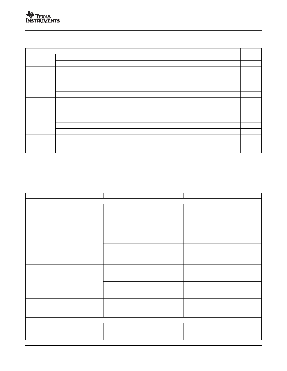
ELECTRICAL CHARACTERISTICS
SLVS710A – JANUARY 2007 – REVISED AUGUST 2007
RECOMMENDED OPERATING CONDITIONS (continued)
over operating free-air temperature range (unless otherwise noted)
MIN
NOM
MAX
UNIT
Output voltage range for LDO1 and LDO2
1
3.6
V
VO
Output voltage range for LDO3 and LDO4
1
3.6
V
Output current at L1 (DCDC1) for TPS65051, TPS65052
1000
mA
Output current at L1 (DCDC1) for TPS65050, TPS65054
600
mA
IO
Output current at L1 (DCDC2)
600
mA
Output current at VLDO1, VLDO2
400
mA
Output current at VLDO3, VLDO4
200
mA
Inductor at L1, L2(1)
1.5
2.2
μH
Output capacitor at VDCDC1, VDCDC2(1)
10
22
μF
CO
Output capacitor at VLDO1, VLDO2, VLDO3, VLDO4(1)
2.2
μF
Input capacitor at VCC(1)
1
μF
CI
Input capacitor at VINLDO1/2(1)
2.2
μF
Input capacitor at VINLDO3/4(1)
2.2
μF
TA
Operating ambient temperature range
-40
85
°C
TJ
Operating junction temperature range
-40
125
°C
Resistor from battery voltage to VCC used for filtering
(2)
1
10
(1)
See the Application Information section of this data sheet for more details.
(2)
Up to 2 mA can flow into VCC when both converters are running in PWM, this resistor causes the UVLO threshold to be shifted
accordingly.
VCC = VINDCDC1/2 = 3.6 V, EN = VCC, MODE = GND, L = 2.2 μH, CO = 10 μF. TA = -40°C to 85°C, typical values are at
TA = 25°C (unless otherwise noted).
PARAMETER
TEST CONDITIONS
MIN
TYP
MAX
UNIT
SUPPLY CURRENT
VI
Input voltage range at VINDCDC1/2
2.5
6
V
One converter, IO = 0 mA.
PFM mode enabled (Mode = GND) device not
20
30
μA
switching, EN_DCDC1 = VI OR EN_DCDC2 = VI;
EN_LDO1= EN_LDO2 = EN_LDO3/4 = GND
Two converters, IO = 0 mA
Operating quiescent current
PFM mode enabled (Mode = 0) device not switching,
32
40
μA
IQ
Total current into VCC, VINDCDC1/2,
EN_DCDC1 = VI AND EN_DCDC2 = VI; EN_LDO1 =
VINLDO1, VINLDO2, VINLDO3/4
EN_LDO2 = EN_LDO3/4 = GND
One converter, IO = 0 mA.
PFM mode enabled (Mode = GND) device not
switching, EN_DCDC1 = VI OR EN_DCDC2 = VI;
180
250
μA
EN_LDO1 = EN_LDO2 = EN_LDO3 = EN_LDO4 =
VI
One converter, IO = 0 mA.
Switching with no load (Mode = VI), PWM operation
0.85
mA
EN_DCDC1 = VI OR EN_DCDC2 = VI; EN_LDO1 =
EN_LDO2 = EN_LDO3/4 = GND
IQ
Operating quiescent current into VCC
Two converters, IO = 0 mA
Switching with no load (Mode = VI), PWM operation
1.25
mA
EN_DCDC1 = VI AND EN_DCDC2 = VI; EN_LDO1 =
EN_LDO2 = EN_LDO3/4 = GND
EN_DCDC1 = EN_DCDC2 = GND EN_LDO1 =
I(SD)
Shutdown current
9
12
μA
EN_LDO2 = EN_LDO3 = EN_LDO4 = GND
Undervoltage lockout threshold for
V(UVLO)
Voltage at VCC
1.8
2
V
DCDC converters and LDOs
EN_DCDC1, EN_DCDC2, DEFDCDC2, DEFLDO1, DEFLDO2, DEFLDO3, DEFLDO4, EN_LDO1, EN_LDO2, EN_LDO3, EN_LDO4
MODE/DATA, EN_DCDC1, EN_DCDC2,
DEFDCDC2, DEFLDO1, DEFLDO2, DEFLDO3,
VIH
High-level input voltage
1.2
VCC
V
DEFLDO4, EN_LDO1, EN_LDO2, EN_LDO3,
EN_LDO4
Copyright 2007, Texas Instruments Incorporated
3
Product Folder Link(s): TPS65050, TPS65051, TPS65052 TPS65054, TPS65056
相關(guān)PDF資料 |
PDF描述 |
|---|---|
| TWA3-48S5 | 1-OUTPUT 2.5 W DC-DC REG PWR SUPPLY MODULE |
| TRU050-GACGA-35M3280000 | PHASE LOCKED LOOP, CDSO16 |
| TRU050-GACGB-27M0000000 | PHASE LOCKED LOOP, CDSO16 |
| TRU050-GACGB-33M3300000 | PHASE LOCKED LOOP, CDSO16 |
| TRU050-GACGB-38M8800000 | PHASE LOCKED LOOP, CDSO16 |
相關(guān)代理商/技術(shù)參數(shù) |
參數(shù)描述 |
|---|---|
| TPS65051RSMT | 功能描述:PMIC 解決方案 6Ch Pwr Mgmt IC RoHS:否 制造商:Texas Instruments 安裝風(fēng)格:SMD/SMT 封裝 / 箱體:QFN-24 封裝:Reel |
| TPS65051RSMTG4 | 功能描述:PMIC 解決方案 6Ch Pwr Mgmt IC RoHS:否 制造商:Texas Instruments 安裝風(fēng)格:SMD/SMT 封裝 / 箱體:QFN-24 封裝:Reel |
| TPS65052EVM-195 | 功能描述:電源管理IC開發(fā)工具 TPS65052-195 Eval Mod RoHS:否 制造商:Maxim Integrated 產(chǎn)品:Evaluation Kits 類型:Battery Management 工具用于評(píng)估:MAX17710GB 輸入電壓: 輸出電壓:1.8 V |
| TPS65052RSMR | 功能描述:PMIC 解決方案 6Ch Pwr Mgmt IC RoHS:否 制造商:Texas Instruments 安裝風(fēng)格:SMD/SMT 封裝 / 箱體:QFN-24 封裝:Reel |
| TPS65052RSMRG4 | 功能描述:PMIC 解決方案 6Ch Pwr Mgmt IC RoHS:否 制造商:Texas Instruments 安裝風(fēng)格:SMD/SMT 封裝 / 箱體:QFN-24 封裝:Reel |
發(fā)布緊急采購(gòu),3分鐘左右您將得到回復(fù)。