- 您現(xiàn)在的位置:買賣IC網(wǎng) > PDF目錄98285 > TPS65150PWPR (TEXAS INSTRUMENTS INC) 3-CHANNEL POWER SUPPLY SUPPORT CKT, PDSO24 PDF資料下載
參數(shù)資料
| 型號: | TPS65150PWPR |
| 廠商: | TEXAS INSTRUMENTS INC |
| 元件分類: | 電源管理 |
| 英文描述: | 3-CHANNEL POWER SUPPLY SUPPORT CKT, PDSO24 |
| 封裝: | GREEN, PLASTIC, HTSSOP-24 |
| 文件頁數(shù): | 28/32頁 |
| 文件大小: | 1412K |
| 代理商: | TPS65150PWPR |
第1頁第2頁第3頁第4頁第5頁第6頁第7頁第8頁第9頁第10頁第11頁第12頁第13頁第14頁第15頁第16頁第17頁第18頁第19頁第20頁第21頁第22頁第23頁第24頁第25頁第26頁第27頁當(dāng)前第28頁第29頁第30頁第31頁第32頁
www.ti.com
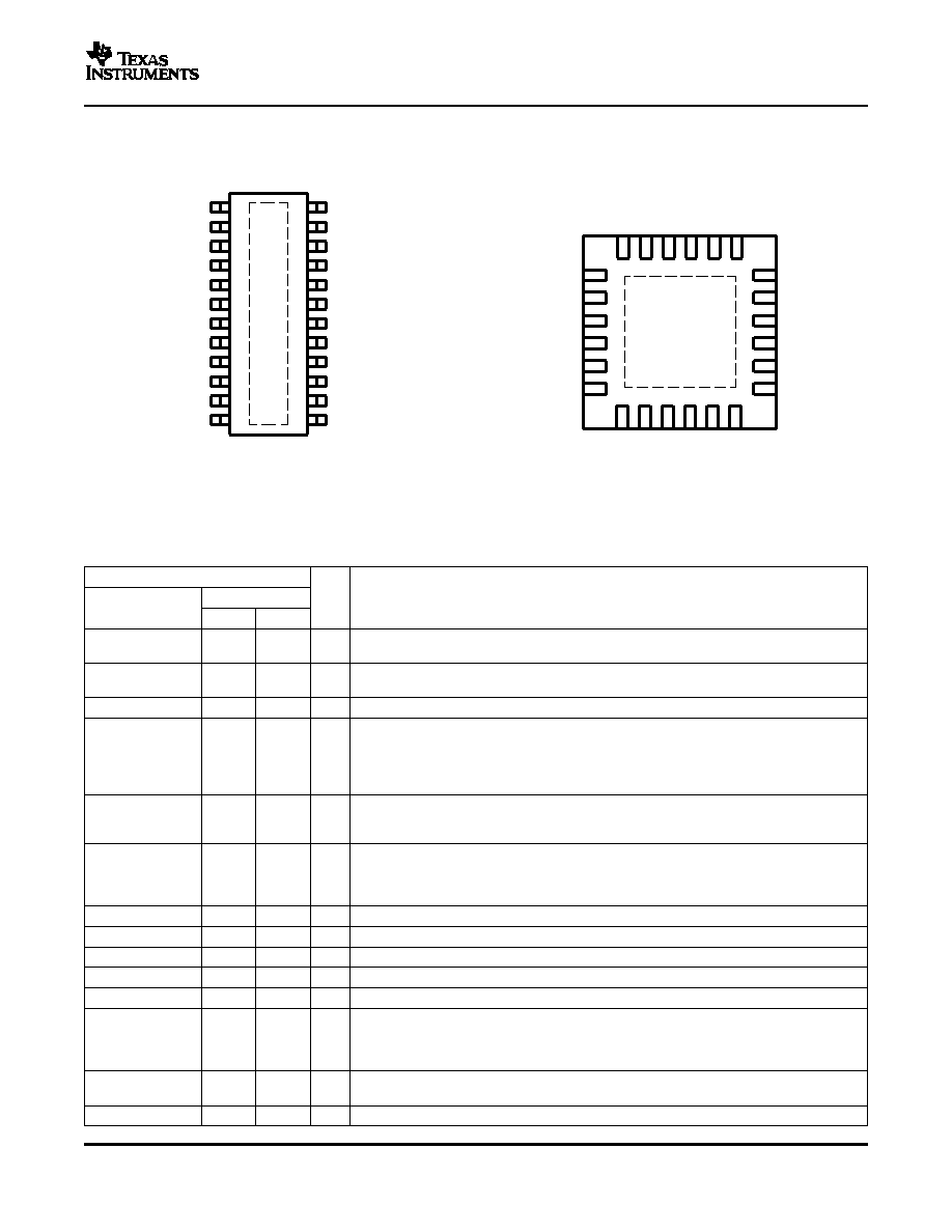
PIN ASSIGNMENT
1
2
3
4
5
6
7
8
9
10
11
12
24
23
22
21
20
19
18
17
16
15
14
13
FB
DLY1
DLY2
VIN
SW
PGND
SUP
VCOM
IN
FBP
FDLY
GD
COMP
FBN
REF
GND
DRVN
DRVP
CPI
VGH
ADJ
CTRL
Thermal
PowerP
AD*
1
2
3
4
5
6
18
17
16
15
14
13
7
8
9
10 11 12
19
20
21
22
23
24
Exposed
Thermal Die*
COMP
GD
FDLY
FB
DLY1
DLY2
VIN
SW
PGND
SUP
VGH
ADJ
CTRL
FBP
IN
VCOM
FBN
REF
GND
DR
VN
DR
VP
CPI
TPS65150
SLVS576 – SEPTEMBER 2005
TSSOP-24 Package
QFN-24 Package
Top View
* The thermal die (PowerPADTM) is connected to GND.
TERMINAL FUNCTIONS
TERMINAL
NO.
I/O
DESCRIPTION
NAME
QFN
TSSOP
Gate voltage shaping circuit. Connecting a capacitor to this pin sets the fall time of the
ADJ
17
14
I/O
positive gate voltage (VGH).
This is the compensation pin for the main boost converter. A small capacitor and if required
COMP
1
22
O
a series resistor is connected to this pin.
CPI
19
16
I
Input of the VGH isolation switch and gate voltage shaping circuit.
Control signal for the gate voltage shaping signal. Apply the control signal for the gate
voltage control. Usually the timing controller of the LCD panel generates this signal. If this
CTRL
16
13
I
function is not required, this pin needs to be connected to VIN. By doing this, the internal
switch between CPI and VGH provides isolation for the positive charge pump output VGH.
DLY2 sets the delay time for VGH to come up.
Power-on sequencing adjust. Connecting a capacitor from this pin to GND allows to set the
DLY1
5
2
I/O
delay time between the boost converter output Vs and the negative charge pump VGL
during startup.
Power-on sequencing adjust. Connecting a capacitor from this pin to GND allows to set the
delay time between the negative charge pump VGL and the positive charge pump during
DLY2
6
3
I/O
startup. Note that Q5 in the Gate Voltage Shaping block only turns on when the positive
charge pump (FBP) is within regulation. (This provides input to output isolation of VGH).
DRVN
21
18
I/O
Charge pump driver to generate the negative voltage VGL.
DRVP
20
17
I/O
Charge pump driver to generate the positive output voltage VGH.
FB
4
1
I
Feedback of the main boost converter generating Vsource (Vs).
FBN
24
21
I
Feedback pin of the negative charge pump VGL.
FBP
15
12
I
Feedback pin of the positive charge pump.
Fault delay. Connecting a capacitor from this pin to Vin allows to set the delay time from
the point when one of the outputs (VS, VGH, VGL) drops below its power good threshold
FDLY
3
24
I/O
until the devices enters the shutdown latch. To re-start the device the input voltage has to
be cycled to GND. This feature can be disabled by connecting the FDLY pin to Vin.
Active low open drain output. This output is latched low when the boost converter Vs is in
GD
2
23
I
regulation. This signal can be used to drive an external MOSFET to provide isolation for Vs.
GND
22
19
Analog ground
5
相關(guān)PDF資料 |
PDF描述 |
|---|---|
| TPS65161APWP | 5.5 A SWITCHING REGULATOR, 900 kHz SWITCHING FREQ-MAX, PDSO28 |
| TPS65161PWPRG4 | 4.2 A SWITCHING REGULATOR, 900 kHz SWITCHING FREQ-MAX, PDSO28 |
| TPS65161BPWP | SWITCHING REGULATOR, 900 kHz SWITCHING FREQ-MAX, PDSO28 |
| TPS65162RGZR | 4.2 A SWITCHING REGULATOR, 900 kHz SWITCHING FREQ-MAX, PQCC48 |
| TPS65167ARHARG4 | 4.9 A SWITCHING REGULATOR, 900 kHz SWITCHING FREQ-MAX, PQCC40 |
相關(guān)代理商/技術(shù)參數(shù) |
參數(shù)描述 |
|---|---|
| TPS65150PWPRG4 | 功能描述:LCD 驅(qū)動(dòng)器 Compact LCD Bias Supply IC RoHS:否 制造商:Maxim Integrated 數(shù)位數(shù)量:4.5 片段數(shù)量:30 最大時(shí)鐘頻率:19 KHz 工作電源電壓:3 V to 3.6 V 最大工作溫度:+ 85 C 最小工作溫度:- 20 C 封裝 / 箱體:PDIP-40 封裝:Tube |
| TPS65150QPWPRQ1 | 制造商:Texas Instruments 功能描述:IC TRIPLE-OUT LCD SPPLY 24HTSSOP 制造商:Texas Instruments 功能描述:3-CH LCD Bias w/ GPM, VCOM Buffer & Gate |
| TPS65150RGER | 功能描述:LCD 驅(qū)動(dòng)器 Compact LCD Bias Supply IC RoHS:否 制造商:Maxim Integrated 數(shù)位數(shù)量:4.5 片段數(shù)量:30 最大時(shí)鐘頻率:19 KHz 工作電源電壓:3 V to 3.6 V 最大工作溫度:+ 85 C 最小工作溫度:- 20 C 封裝 / 箱體:PDIP-40 封裝:Tube |
| TPS65150RGERG4 | 功能描述:LCD 驅(qū)動(dòng)器 Compact LCD Bias Supply IC RoHS:否 制造商:Maxim Integrated 數(shù)位數(shù)量:4.5 片段數(shù)量:30 最大時(shí)鐘頻率:19 KHz 工作電源電壓:3 V to 3.6 V 最大工作溫度:+ 85 C 最小工作溫度:- 20 C 封裝 / 箱體:PDIP-40 封裝:Tube |
| TPS65154RSLR | 制造商:Texas Instruments 功能描述:IC TRIPLE-OUT LCD SUPPLY 48VQFN |
發(fā)布緊急采購,3分鐘左右您將得到回復(fù)。