- 您現(xiàn)在的位置:買賣IC網(wǎng) > PDF目錄373684 > TQ5132 (TRIQUINT SEMICONDUCTOR INC) 3V Cellular Band CDMA/AMPS RFA/Mixer IC PDF資料下載
參數(shù)資料
| 型號(hào): | TQ5132 |
| 廠商: | TRIQUINT SEMICONDUCTOR INC |
| 元件分類: | 無繩電話/電話 |
| 英文描述: | 3V Cellular Band CDMA/AMPS RFA/Mixer IC |
| 中文描述: | TELECOM, CELLULAR, RF FRONT END CIRCUIT, PDSO8 |
| 封裝: | PLASTIC, SOT-23, 8 PIN |
| 文件頁數(shù): | 8/12頁 |
| 文件大小: | 101K |
| 代理商: | TQ5132 |
TQ5132
Data Sheet
8
For additional information and latest specifications, see our website:
www.triquint.com
CDMA IF Amplifier
The CDMA IF amplifier is an open drain stage with a gain step
to adjust the output power levels according to the system
requirement. No quiescent current adjustments are possible in
this mode since the self-bias circuit is on-chip. While the IF
output can be tuned for frequencies as high as 500 MHz, the
downconverter performance is limted by the internal tuned
circuit of the LO buffer amplifier. The highest IF that can be used
without significant deviation fromtypical performance is 130
MHz. This output is a high impedance open drain FET
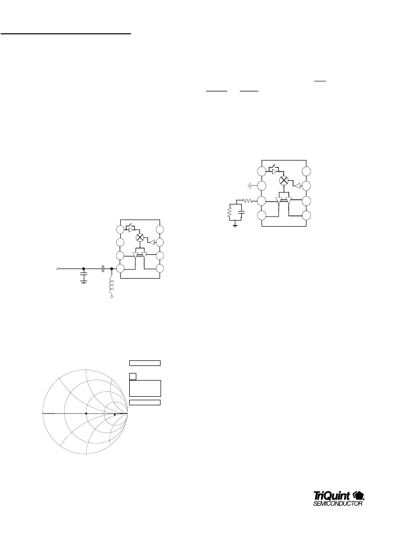
z = 5.47
– j 0.71
(normalized). The match requires a RF choke to Vdd
for proper biasing (see figure 3). Typical CDMA IF output
impedance is shown in figure 4. The gain of the CDMA IF
amplifier can be adjusted according to the degeneration resistor
value R2 (see figure 5).
Note: These values were optimized for TriQuint's 5131 Demo
board. The discrepancy between these values and those of the
customer's application may differ due to board and component
parasitics.
Vdd
L2=180nH
2
1
4
5
6
8
3
7
CDMA
IF
Output
TQ5132
C7
=30pF
C6=27pF
Figure 3. TQ5132 CDMA IF Output Match (IF = 85MHz)
2.0
1.0
0.5
-0.5
-1.0
-2.0
1.0
2.0
0.5
B
0.70 @ -2.8
z = 5.47- j 0.71
y = 0.18 + j 0.02
B
CDIF output
Impedance
TQ5132
Freq=85MHz
Figure 4. TQ5132 CDMA IF Output Impedance at Pin 4
AMPS IF Amplifier
The source of the AMPS IF amplifier is connected directly to pin
3. This allows the systemdesigner to adjust Gain, output
Intercept and Current (GIC) by adding an external self-bias
circuit at this pin (see figure 5). A large bypass capacitor value
in the self-bias circuit mnimzes the effects of low frequency
components present at this pin. TriQuint recommends 0.022uF
or greater. The AMPS IF amplifier gain is only mldly affected by
the value of R2.
Note: These values were optimized for TriQuint's 5131 Demo
board. The discrepancy between these values and those of the
customer's application may differ due to board and component
parasitics.
2
1
4
5
6
8
3
7
TQ5132
C4 = 0.022uF
R2
R3
C4
R2 = 6.8
R3 = 180
Figure 5. TQ5132 AMPS GIC pin
Once the operating point is chosen, the designer still has
flexibility to adjust gain and intercept by varying the ratio of the
DC bias resistors, R2/R3. Maximumgain is obtained when the
total DC resistance (R2 + R3) at pin 3 is bypassed.
The normalized impedance of the AMPS IF output is
z = 15.4 – j
2.87
. This particular measurement was taken on the 5132
demo board by lifting pin 5 of the PCB pad and soldering the
center conductor of a semrigid probe next to it. The outer
conductor was grounded close to the pin and its electrical length
dialed as a port extension in order to move the calibration
reference plane right at the tip of the probe. Keep in mnd that
the total DC bias resistance in the GIC pin must be selected
before taking this measurement. When designing the PCB, it is
recommended to place the self-bias circuit of the amplifier as
close to the pin as possible to mnimze possible loading effects
that mght cause oscillation. Simlarly, the shunt capacitor C10
相關(guān)PDF資料 |
PDF描述 |
|---|---|
| TQ5139 | 2.8V SiGe Dual-Mode CDMA Rx Receiver |
| TQ5622 | 3V PCS Receiver IC With Power- Down |
| TQ5631 | 3V PCS Band CDMA RFA/Mixer IC |
| TQ5633 | 3V PCS Band CDMA RFA/Mixer IC(WIRELESS COMMUNICATIONS DIVISION) |
| TQ5635 | 3 V PCS LNA/Mixer Receiver IC |
相關(guān)代理商/技術(shù)參數(shù) |
參數(shù)描述 |
|---|---|
| TQ5135 | 制造商:TRIQUINT 制造商全稱:TriQuint Semiconductor 功能描述:3V Cellular CDMA/AMPS LNA/Mixer Receiver IC |
| TQ5139 | 制造商:TRIQUINT 制造商全稱:TriQuint Semiconductor 功能描述:2.8V SiGe Dual-Mode CDMA Rx Receiver |
| TQ516-11A-AMINN500 | 功能描述:電線鑒定 VOID LABELS REORDER # AP1878 RoHS:否 制造商:TE Connectivity / Q-Cees 產(chǎn)品:Labels and Signs 類型: 材料:Vinyl 顏色:Blue 寬度:0.625 in 長(zhǎng)度:1 in |
| TQ5622 | 制造商:TRIQUINT 制造商全稱:TriQuint Semiconductor 功能描述:3V PCS Receiver IC With Power- Down |
| TQ5631 | 功能描述:射頻放大器 CDMA High Band Mixer RoHS:否 制造商:Skyworks Solutions, Inc. 類型:Low Noise Amplifier 工作頻率:2.3 GHz to 2.8 GHz P1dB:18.5 dBm 輸出截獲點(diǎn):37.5 dBm 功率增益類型:32 dB 噪聲系數(shù):0.85 dB 工作電源電壓:5 V 電源電流:125 mA 測(cè)試頻率:2.6 GHz 最大工作溫度:+ 85 C 安裝風(fēng)格:SMD/SMT 封裝 / 箱體:QFN-16 封裝:Reel |
發(fā)布緊急采購,3分鐘左右您將得到回復(fù)。