- 您現(xiàn)在的位置:買賣IC網(wǎng) > PDF目錄378718 > TRSL-9380G (Optoway Technology Inc.) 3.3V / 1550 nm / 2.5 Gbps RoHS Compliant SFF LC SINGLE-MODE TRANSCEIVER PDF資料下載
參數(shù)資料
| 型號: | TRSL-9380G |
| 廠商: | Optoway Technology Inc. |
| 英文描述: | 3.3V / 1550 nm / 2.5 Gbps RoHS Compliant SFF LC SINGLE-MODE TRANSCEIVER |
| 中文描述: | 3.3 / 1550海里/ 2.5 Gbps的符合RoHS準系統(tǒng)立法會單模收發(fā)器 |
| 文件頁數(shù): | 3/4頁 |
| 文件大小: | 123K |
| 代理商: | TRSL-9380G |
TRSL-9380
**********************************************************************************************************************************************************************
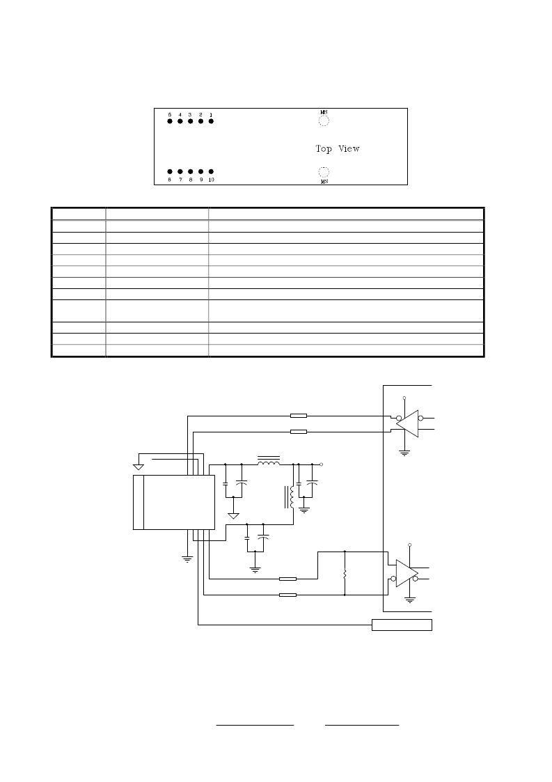
CONNECTION DIAGRAM
**********************************************************************************************************************************************************************
OPTOWAY TECHNOLOGY INC.
No
.3
8, Kuang Fu S. Road, Hu Kou, Hsin Chu Industrial Park, Hsin Chu, Taiwan 303
Tel: 886-3-5979798 Fax: 886-3-5979737
E-mail: sales@optoway.com.tw http: // www.optoway.com.tw 12/1/2005 V2.0
3
PIN
1
2
3
4
5
6
7
8
Symbol
V
EE
r
V
CC
r
SD
RD
RD+
V
CC
t
V
EE
t
TxDis
Notes
Directly connect this pin to the receiver ground plane
+3.3V dc power for the receiver section
Active high on this indicates a received optical signal.
Receiver Dataout Bar. See recommended circuit schematic
Receiver Dataout. See recommended circuit schematic
+3.3V dc power for the transmitter section
Directly connect this plan to the transmitter ground plane
Transmitter Disable. Connect this pin to +3.3V TTL logic
“
1
”
to disable module
To enable module connect to TTL logic low
“
0
”
Transmitter Data In. See recommended circuit schematic
Transmitter Data In Bar. See recommended circuit schematic
Mounting Studs. Connect to Chassis Ground
9
10
MS
TD+
TD-
MS
RECOMMENDED CIRCUIT SCHEMATIC
V
1
V
2
S
3
R
4
R
5
V
6
V
7
T
8
T
9
T
1
TXDis(LVTTL)
Z=5OR
Z=50R
1uH
10uF
10nF
10uF
10nF
Vcc3.3V
1uH
10uF
10nF
Z=5OR
Z=50R
PHY DEVICE
TD-
TD+
RD+
RD-
SD
100R
Vcc3.3V
LVPECL
Vcc3.3V
LVPECL
TO LVTTL STAGE
Note: 1. TX input is termnated inside the module.
2. Veer and Veet are not internally connected to each other.
3. 50
Ω
line pattern and component placements on TD+/TD- and RD+/RD- lines shall be symmetrical for
better impedance matching.
相關PDF資料 |
PDF描述 |
|---|---|
| TSAL5100 | LED IrLED 940nm 2-Pin T-1 3/4 Bulk |
| TSAL5300 | LED IrLED 940nm 2-Pin T-1 3/4 Bulk |
| TSAL6400 | LED IrLED 950nm 2-Pin T-1 3/4 Bulk |
| TSAL7300 | LED IrLED 940nm 2-Pin T-1 3/4 Bulk |
| TSHA5500 | LED IrLED 875nm 2-Pin T-1 3/4 Bulk |
相關代理商/技術參數(shù) |
參數(shù)描述 |
|---|---|
| TRSL-9380G_11 | 制造商:OPTOWAY 制造商全稱:Optoway Technology Inc 功能描述:3.3V / 1550 nm / 2.5 Gbps RoHS Compliant SFF LC SINGLE-MODE TRANSCEIVER |
發(fā)布緊急采購,3分鐘左右您將得到回復。