- 您現(xiàn)在的位置:買賣IC網(wǎng) > PDF目錄98307 > TWL1106PWR (TEXAS INSTRUMENTS INC) SPECIALTY CONSUMER CIRCUIT, PDSO20 PDF資料下載
參數(shù)資料
| 型號: | TWL1106PWR |
| 廠商: | TEXAS INSTRUMENTS INC |
| 元件分類: | 消費(fèi)家電 |
| 英文描述: | SPECIALTY CONSUMER CIRCUIT, PDSO20 |
| 封裝: | PLASTIC, TSSOP-20 |
| 文件頁數(shù): | 17/19頁 |
| 文件大小: | 260K |
| 代理商: | TWL1106PWR |

TWL1106
VOICEBAND AUDIO PROCESSOR (VBAP)
SLWS094 – JUNE 2001
7
POST OFFICE BOX 655303
DALLAS, TEXAS 75265
electrical characteristics over recommended ranges of supply voltage and operating free-air temperature
(unless otherwise noted) (continued)
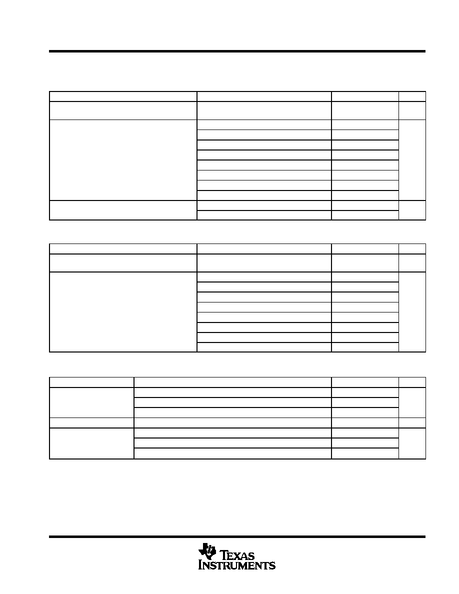
transmit idle channel noise and distortion, companded mode (
-law) selected
PARAMETER
TEST CONDITIONS
MIN
TYP
MAX
UNIT
Transmit idle channel noise, psophometrically
weighted
MIC Amp 1 configured for 23.5 dB gain
(see Note 8)
–80
–70
dBm0p
MICIN–, MICIN+ to PCMO at 3 dBm0
27
MICIN–, MICIN+ to PCMO at 0 dBm0
30
MICIN–, MICIN+ to PCMO at –5 dBm0
33
Transmit signal-to-distortion ratio with
MICIN–, MICIN+ to PCMO at –10 dBm0
36
dBm0
Transmit signal to distortion ratio with
1.02-kHz sine-wave input
MICIN–, MICIN+ to PCMO at –20 dBm0
35
dBm0
MICIN–, MICIN+ to PCMO at –30 dBm0
26
MICIN–, MICIN+ to PCMO at –40 dBm0
24
MICIN–, MICIN+ to PCMO at –45 dBm0
19
Intermodulation distortion, 2-tone CCITT method,
CCITT G.712 (7.1), R2
49
dB
Intermodulation distortion, 2 tone CCITT method,
composite power level, –13 dBm0
CCITT G.712 (7.2), R2
51
dB
NOTE 8: With recommended impedances and resistor tolerance of 1%
transmit idle channel noise and distortion, linear mode selected
PARAMETER
TEST CONDITIONS
MIN
TYP
MAX
UNIT
Transmit idle channel noise, psophometrically
weighted
MIC Amp 1 configured for 23.5 dB gain
(see Note 8)
–80
–74
dBm0p
MICIN–, MICIN+ to PCMO at 3 dBm0
40
55
MICIN–, MICIN+ to PCMO at 0 dBm0
50
61
MICIN–, MICIN+ to PCMO at –5 dBm0
52
62
Transmit signal-to-total distortion ratio with 1.02-kHz
MICIN–, MICIN+ to PCMO at –10 dBm0
56
66
dB
Transmit signal to total distortion ratio with 1.02 kHz
sine-wave input
MICIN–, MICIN+ to PCMO at –20 dBm0
52
68
dB
MICIN–, MICIN+ to PCMO at –30 dBm0
51
61
MICIN–, MICIN+ to PCMO at –40 dBm0
43
59
MICIN–, MICIN+ to PCMO at –45 dBm0
38
55
NOTE 8: With recommended impedances and resistor tolerance of 1%
receive gain and dynamic range, linear or companded (
-law) mode selected (see Note 9)
PARAMETER
TEST CONDITIONS
MIN
TYP
MAX
UNIT
Load = 8
, volume control = –3 dB, PCMI data input to –4 dB level
3.20
Overload-signal level (3 dB)
Load = 16
, volume control = –3 dB, PCMI data input to –2 dB level
4.05
Vpp
Overload signal level (3 dB)
Load = 32
, volume control = –3 dB, PCMI data input to –1 dB level
4.54
V
Absolute gain error
0 dBm0 input signal, 2.7 V
≤ VDD ≤ 3.3 V
–1
1
dB
G i
ith
t
t l
l
PCMI to EAROUT–, EAROUT+ at 3 dBm0 to –40 dBm0
–0.5
0.5
Gain error with output level
relative to gain at –10 dBm0
PCMI to EAROUT–, EAROUT+ at –41 dBm0 to –50 dBm0
–1
1
dB
relative to gain at –10 dBm0
PCMI to EAROUT–, EAROUT+ at –51 dBm0 to –55 dBm0
–1.2
1.2
dB
NOTE 9: 1020-Hz input signal at PCMI, output measured differentially between EAROUT– and EAROUT+
相關(guān)PDF資料 |
PDF描述 |
|---|---|
| TWL1106PW | SPECIALTY CONSUMER CIRCUIT, PDSO20 |
| TWL1107PWR | SPECIALTY CONSUMER CIRCUIT, PDSO20 |
| TWL1107PW | SPECIALTY CONSUMER CIRCUIT, PDSO20 |
| TWL1110GQE | SPECIALTY CONSUMER CIRCUIT, PBGA80 |
| TWL1110PBSR | SPECIALTY CONSUMER CIRCUIT, PQFP32 |
相關(guān)代理商/技術(shù)參數(shù) |
參數(shù)描述 |
|---|---|
| TWL1107 | 制造商:TI 制造商全稱:Texas Instruments 功能描述:VOICE-BAND AUDIO PROCESSOR (VBAP?£a) |
| TWL1107PW | 制造商:未知廠家 制造商全稱:未知廠家 功能描述: |
| TWL1107PWR | 制造商:Rochester Electronics LLC 功能描述:- Bulk |
| TWL1109 | 制造商:TI 制造商全稱:Texas Instruments 功能描述:VOICE-BAND AUDIO PROCESSOR VBAPE |
| TWL1109PBS | 制造商:TI 制造商全稱:Texas Instruments 功能描述:VOICE-BAND AUDIO PROCESSOR VBAPE |
發(fā)布緊急采購,3分鐘左右您將得到回復(fù)。