- 您現(xiàn)在的位置:買(mǎi)賣(mài)IC網(wǎng) > PDF目錄379464 > UA733N 96KHZ DIGITAL AUDIO INTERFACE TRANSMITTER PDF資料下載
參數(shù)資料
| 型號(hào): | UA733N |
| 英文描述: | 96KHZ DIGITAL AUDIO INTERFACE TRANSMITTER |
| 中文描述: | 單視頻放大器 |
| 文件頁(yè)數(shù): | 3/16頁(yè) |
| 文件大?。?/td> | 486K |
| 代理商: | UA733N |
第1頁(yè)第2頁(yè)當(dāng)前第3頁(yè)第4頁(yè)第5頁(yè)第6頁(yè)第7頁(yè)第8頁(yè)第9頁(yè)第10頁(yè)第11頁(yè)第12頁(yè)第13頁(yè)第14頁(yè)第15頁(yè)第16頁(yè)
The
and no longer supplied.
A733M is obsolete
SLFS027B NOVEMBER 1970 REVISED MAY 2004
3
POST OFFICE BOX 655303
DALLAS, TEXAS 75265
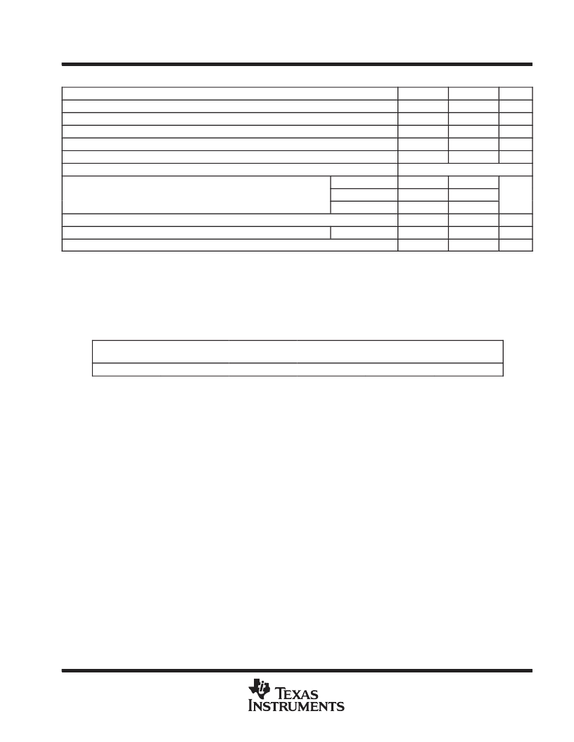
absolute maximum ratings over operating free-air temperature range (unless otherwise noted)
A733C
A733M
UNIT
Supply voltage VCC+ (see Note 1)
Supply voltage VCC (see Note 1)
Differential input voltage
8
8
V
8
±
5
±
6
10
8
±
5
±
6
10
V
V
Common-mode input voltage
V
Output current
mA
Continuous total power dissipation
See Dissipation Rating Table
D package
86
Package thermal impedance, JA (see Notes 2 and 3)
N package
80
°
C/W
NS package
76
Maximum junction temperature, TJ
Lead temperature 1,6 mm (1/16 inch) from case for 60 seconds
150
°
C
°
C
°
C
J or U package
300
Storage temperature range, Tstg
Stresses beyond those listed under absolute maximum ratings may cause permanent damage to the device. This is a stress rating only, and
functional operation of the device at these or any other conditions beyond those indicated in the recommended operating conditions section of
this specification is not implied. Exposure to absolute-maximum-rated conditions for extended periods may affect device reliability.
NOTES:
1. All voltage values, except differential input voltages, are with respect to the midpoint between VCC+ and VCC–.
2. Maximum power dissipation is a function of TJ(max), JA, and TA. The maximum allowable power dissipation at any allowable
ambient temperature is PD = (TJ(max) – TA)/JA. Operating at the absolute maximum TJ of 150
°
C can affect reliability.
3. The package thermal impedance is calculated in accordance with JESD 51-7.
65 to 150
65 to 150
DISSIPATION RATING TABLE
PACKAGE
TA
≤
25
°
C
POWER RATING
DERATING
FACTOR
DERATE
ABOVE TA
104
°
C
TA = 70
°
C
POWER RATING
TA = 125
°
C
POWER RATING
J (
μ
A733M)
500 mW
11.0 mW/
°
C
500 mW
269 mW
相關(guān)PDF資料 |
PDF描述 |
|---|---|
| UA733N-B | Digital audio interface receiver |
| UA733M | DIFFERENTIAL VIDEO AMPLIFIERS |
| UA741IP | GENERAL-PURPOSE OPERATIONAL AMPLIFIERS |
| UA741UFK | GENERAL-PURPOSE OPERATIONAL AMPLIFIERS |
| UA741UFKB | GENERAL-PURPOSE OPERATIONAL AMPLIFIERS |
相關(guān)代理商/技術(shù)參數(shù) |
參數(shù)描述 |
|---|---|
| UA733N-B | 制造商:未知廠家 制造商全稱:未知廠家 功能描述:Single Video Amplifier |
| UA734 | 制造商:FAIRCHILD 制造商全稱:Fairchild Semiconductor 功能描述:PRECISION VOLTAGE COMPARATOR |
| UA734C | 制造商:FAIRCHILD 制造商全稱:Fairchild Semiconductor 功能描述:PRECISION VOLTAGE COMPARATOR |
| UA734HC | 制造商:FAIRCHILD 制造商全稱:Fairchild Semiconductor 功能描述:PRECISION VOLTAGE COMPARATOR |
| UA734HM | 制造商:FAIRCHILD 制造商全稱:Fairchild Semiconductor 功能描述:PRECISION VOLTAGE COMPARATOR |
發(fā)布緊急采購(gòu),3分鐘左右您將得到回復(fù)。