- 您現(xiàn)在的位置:買賣IC網(wǎng) > PDF目錄379475 > UC1625N (Texas Instruments, Inc.) Brushless DC Motor Controller PDF資料下載
參數(shù)資料
| 型號(hào): | UC1625N |
| 廠商: | Texas Instruments, Inc. |
| 英文描述: | Brushless DC Motor Controller |
| 中文描述: | 無刷直流電機(jī)控制器 |
| 文件頁數(shù): | 2/15頁 |
| 文件大小: | 313K |
| 代理商: | UC1625N |
2
UC1625
UC2625
UC3625
V
CC
Supply Voltage. . . . . . . . . . . . . . . . . . . . . . . . . . . . . . +20V
Pwr V
CC
Supply Voltage . . . . . . . . . . . . . . . . . . . . . . . . . . +20V
PWM In . . . . . . . . . . . . . . . . . . . . . . . . . . . . . . . . . . . –0.3 to 6V
E/A IN(+), E/A IN(–). . . . . . . . . . . . . . . . . . . . . . . . . –0.3 to 12V
I
SENSE1
, I
SENSE2
. . . . . . . . . . . . . . . . . . . . . . . . . . . . . –1.3 to 6V
OV–Coast, Dir, Speed-In, S
START
, Quad Sel . . . . . . –0.3 to 8V
H1, H2, H3. . . . . . . . . . . . . . . . . . . . . . . . . . . . . . . . –0.3 to 12V
PU Output Voltage. . . . . . . . . . . . . . . . . . . . . . . . . . –0.3 to 50V
PU Output Current . . . . . . . . . . . . . . . . . . +200 mA continuous
PD Output Current . . . . . . . . . . . . . . . . . .
±
200 mA continuous
E/A Output Current . . . . . . . . . . . . . . . . . . . . . . . . . . . .
±
10 mA
I
SENSE
Output Current . . . . . . . . . . . . . . . . . . . . . . . . . . –10 mA
Tach Out Output Current. . . . . . . . . . . . . . . . . . . . . . . .
±
10 mA
V
REF
Output Current . . . . . . . . . . . . . . . . . . –50 mA continuous
Operating Temperature Range UC1625. . . . . . –55°C to 125°C
Operating Temperature Range UC2625. . . . . . –40°C to 105°C
Operating Temperature Range UC3625. . . . . . . . . 0°C to 70°C
Note 1:
Currents are positive into and negative out of the spec-
ified terminal.
Note 2:
Consult Unitrode Integrated Circuits databook for infor-
mation regarding thermal specifications and limitations
of packages.
ABSOLUTE MAXIMUM RATINGS
ELECTRICAL CHARACTERISTICS:
Unless otherwise stated, these specifications apply for: T
A
= 25
°
C; Pwr V
CC
= V
CC
= 12V;
R
OSC=
20k to V
REF
; C
OSC
= 2nF; R
TACH
= 33k; C
TACH
= 10nF; and all outputs unloaded. T
A
= T
J.
PARAMETER
TEST CONDITIONS
Overall
Supply current
Over Operating Range
V
CC
Turn-On Threshold
Over Operating Range
V
CC
Turn-Off Threshold
Over Operating Range
Overvoltage/Coast
OV-Coast Inhibit Threshold
Over Operating Range
OV-Coast Restart Threshold
OV-Coast Hysteresis
OV-Coast Input Current
Logic Inputs
H1, H2, H3 Low Threshold
Over Operating Range
H1, H2, H3 High Threshold
Over Operating Range
H1, H2, H3 Input Current
Over Operating Range, to 0V
Quad Sel, Dir Thresholds
Over Operating Range
Quad Sel Hysteresis
Dir Hysteresis
Quad Sel Input Current
Dir Input Current
PWM Amp/Comparator
E/A In(+), E/A In(–) Input Current
To 2.5V
PWM In Input Current
To 2.5V
Error Amp Input Offset
0V < V
COMMON-MODE
< 3V
Error Amp Voltage Gain
MIN
TYP
MAX
UNITS
14.5
8.95
8.05
30.0
9.45
8.55
mA
V
V
8.65
7.75
1.65
1.55
0.05
–10
1.75
1.65
0.10
–1
1.85
1.75
0.15
0
V
V
V
μ
A
0.8
1.6
-400
0.8
1.0
1.9
-250
1.4
70
0.6
50
–1
1.2
2.0
–120
2.0
V
V
μ
A
V
mV
V
μ
A
μ
A
–30
–30
150
30
–5.0
0
–10
70
–0.1
3
5.0
30
10
μ
A
μ
A
mV
dB
90
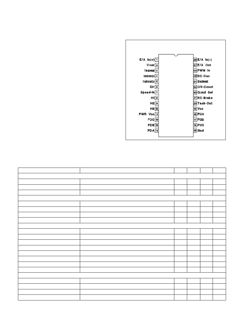
CONNECTION DIAGRAM
Note 3:
This pinout applies to the SOIC (DW), PLCC (Q), and
LCC (L) packages (ie. pin 22 has the same function on all
packages.)
DIL-28 (TOP VIEW)
J or N PACKAGE
相關(guān)PDF資料 |
PDF描述 |
|---|---|
| UC3711J | Dual Ultra High-Speed FET Driver |
| UC382TDTR-2 | 3A Fixed Low Dropout Linear Regulator (LDO) |
| UC2825BQTR | Double channel high side driver with analog current sense for automotive applications |
| UC2825L | Double channel high side driver for automotive applications |
| UC2826DW | Double channel high side driver for automotive applications |
相關(guān)代理商/技術(shù)參數(shù) |
參數(shù)描述 |
|---|---|
| UC1625-SP | 制造商:TI 制造商全稱:Texas Instruments 功能描述:RAD-TOLERANT CLASS V, BRUSHLESS DC MOTOR CONTROLLER |
| UC1633 | 制造商:TI 制造商全稱:Texas Instruments 功能描述:Phase Locked Frequency Controller |
| UC1633 WAF | 制造商:Texas Instruments 功能描述: |
| UC1633J883BS | 制造商:Texas Instruments 功能描述:- Rail/Tube |
| UC1633L | 制造商:Texas Instruments 功能描述:FREQUENCY CONTROLLER - Rail/Tube |
發(fā)布緊急采購(gòu),3分鐘左右您將得到回復(fù)。